2 extended feature set application schematic – Rainbow Electronics AT86RF231 User Manual
Page 14
14
8111A–AVR–05/08
AT86RF231
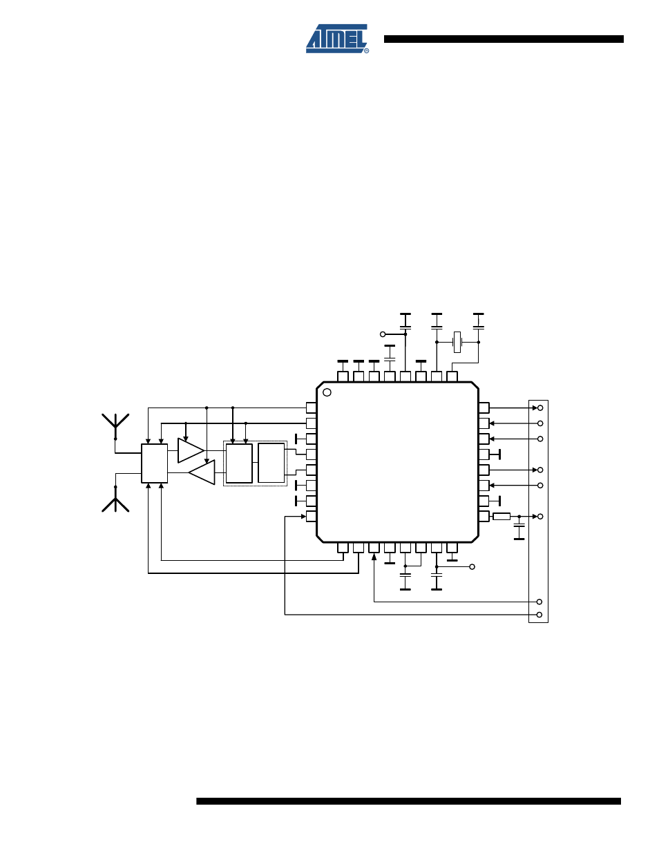
5.2
Extended Feature Set Application Schematic
The AT86RF231 supports additional features like:
An extended feature set application schematic illustrating the use of the AT86RF231 Extended
Feature Set, see
Section 11. “AT86RF231 Extended Feature Set” on page 128
, is shown in
. Although this example shows all additional hardware features combined, it
is possible to use all features separately or in various combinations.
Figure 5-2.
Extended Feature Application Schematic
In this example, a balun (B1) transforms the differential RF signal at the radio transceiver RF
pins (RFP/RFN) to a single ended RF signal, similar to the Basic Application Schematic; refer to
. The RF-Switches (SW1, SW2) separate between receive and transmit
path in an external RF front-end.
These switches are controlled by the RX/TX Indicator, represented by the differential pin pair
DIG3/DIG4, refer to
Section 11.5 “RX/TX Indicator” on page 147
.
During receive the radio transceiver searches for the most reliable RF signal path using the
Antenna Diversity algorithm. One antenna is selected (SW2) by the Antenna Diversity RF switch
•
Security Module (AES)
see
•
High Data Rate Mode
see
•
Antenna Diversity
uses pins DIG1/2
see
•
RX/TX indicator
uses pins DIG3/4
see
•
RX Frame Time Stamp
uses pin DIG2
see
8
7
6
5
4
3
2
1
9
10
11
12
13
14
15
16
25
26
27
28
29
30
31
32
AT86RF231
DIG3
AVSS
DIG4
A
VSS
AVSS
RFP
RFN
AVSS
DVSS
DI
G1
DI
G2
SLP_
T
R
D
VSS
DV
D
D
DV
D
D
XT
AL
2
D
EVD
D
D
VSS
AVSS
AV
DD
EV
D
D
A
VSS
XT
AL
1
17
18
19
20
21
22
23
24
DVSS
CLKM
IRQ
MISO
DVSS
MOSI
SCLK
CB3
CB4
XTAL
CX1
CX2
CB1
Digita
l Int
e
rf
ac
e
V
DD
/RST
/SEL
Balun
RF-
Sw
it
ch
ANT0
ANT1
RF-
Sw
it
ch
B1
SW1
SW2
V
DD
CB2
C3
R1
PA
LNA
N1
N2