Rainbow Electronics RF12B User Manual
Rf12b universal ism band fsk transceiver, Rf12b
RF12B
RF12B Universal ISM Band
FSK Transceiver
Tel: +86-755-86096587 Fax: +86-755-86096602 E-mail: [email protected] http://www.hoperf.com
DESCRIPTION
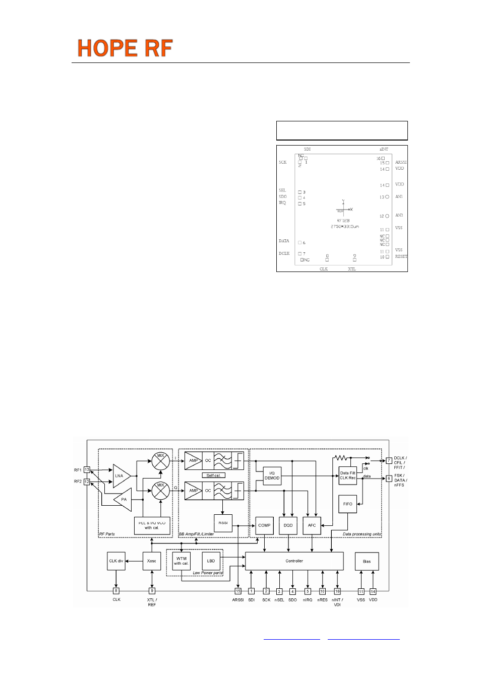
Hope’s RF12B is a single chip, low power,
multi-channel FSK transceiver designed for use in
applications requiring FCC or ETSI conformance for
unlicensed use in the 433, 868 and 915 MHz bands. The
RF12B transceiver produces a flexible, low cost, and highly
integrated solution that does not require production
alignments. The chip is a complete analog RF and baseband
transceiver including a multi-band PLL synthesizer with PA,
LNA, I/Q down converter mixers, baseband filters and
amplifiers, and an I/Q demodulator. All required RF functions
are integrated. Only an external crystal and bypass filtering
are needed for operation.
RF12B
The RF12B features a completely integrated PLL for easy RF design, and its rapid settling time
allows for fast frequency-hopping, bypassing multi-path fading and interference to achieve robust
wireless links. The PLL’s high resolution allows the usage of multiple channels in any of the bands. The
receiver baseband bandwidth (BW) is programmable to accommodate various deviation, data rate and
crystal tolerance requirements. The transceiver employs the Zero-IF approach with I/Q demodulation.
Consequently, no external components (except crystal and decoupling) are needed in most applications.
The RF12B dramatically reduces the load on the microcontroller with the integrated digital data
processing features: data filtering, clock recovery, data pattern recognition, integrated FIFO and TX data
register. The automatic frequency control (AFC) feature allows the use of a low accuracy (low cost)
crystal. To minimize the system cost, the RF12B can provide a clock signal for the microcontroller,
avoiding the need for two crystals.
For low power applications, the RF12B supports low duty cycle operation based on the internal
wake-up timer.
FUNCTIONAL BLOCK DIAGRAM
Document Outline
- FEATURES
- TYPICAL APPLICATIONS
- DETAILED FEATURE-LEVEL DESCRIPTION
- PACKAGE PIN DEFINITIONS
- Typical Application
- GENERAL DEVICE SPECIFICATION
- ELECTRICAL SPECIFICATION
- CONTROL INTERFACE
- TX REGISTER BUFFERED DATA TRANSMISSION
- RX FIFO BUFFERED DATA READ
- CRYSTAL SELECTION GUIDELINES
- RX-TX ALIGNMENT PROCEDURES
- TYPICAL PERFORMANCE CHARACTERISTICS
- REFERENCE DESIGNS
- SGS Reports
- RF12B BONDING DIAGRAM