Rainbow Electronics AT86RF231 User Manual
Page 13
13
8111A–AVR–05/08
AT86RF231
the reference frequency, large parasitic capacitances should be avoided. Crystal lines should be
routed as short as possible and not in proximity of digital I/O signals. This is especially required
for the High Data Rate Modes, refer to
Section 11.3 “High Data Rate Modes” on page 137
Crosstalk from digital signals on the crystal pins or the RF pins can degrade the system perfor-
mance. Therefore, a low-pass filter (C3, R1) is placed close to the CLKM output pin to reduce
the emission of CLKM signal harmonics. This is not needed if the CLKM pin is not used as a
microcontroller clock source. In that case, the output should be turned off during device
initialization.
The ground plane of the application board should be separated into four independent fragments,
the analog, the digital, the antenna and the XTAL ground plane. The exposed paddle shall act as
the reference point of the individual grounds.
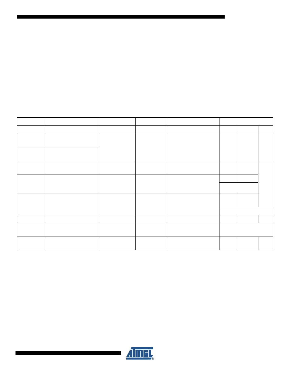
Table 5-1.
Example Bill of Materials (BoM) for Basic Application Schematic
Designator
Description
Value
Manufacture
Part Number
Comment
B1
SMD balun
2.4 GHz
Wuerth
748421245
CB1
CB3
LDO VREG
bypass capacitor
1 µF
AVX
Murata
0603YD105KAT2A
GRM188R61C105KA12D
X5R
(0603)
10%
16V
CB2
CB4
Power Supply decoupling
CX1, CX2
Crystal load capacitor
12 pF
AVX
Murata
06035A120JA
GRP1886C1H120JA01
COG
(0603)
5%
50V
C1, C2
RF coupling capacitor
22 pF
Epcos
Epcos
AVX
B37930
B37920
06035A220JAT2A
COG
5%
(0402 or 0603)
C3
CLKM low-pass
filter capacitor
2.2 pF
AVX
Murata
06035A229DA
GRP1886C1H2R0DA01
COG
(0603)
±0.5 pF
Designed for f
CLKM
=1 MHz
C4
RF matching
0.47 pF
Johnstech
R1
CLKM low-pass
filter resistor
680
Ω
Designed for f
CLKM
=1 MHz
XTAL
Crystal
CX-4025 16 MHz
SX-4025 16 MHz
ACAL Taitjen
Siward
XWBBPL-F-1
A207-011