4 basic operating mode timing, 1 power-on procedure – Rainbow Electronics AT86RF231 User Manual
Page 39
39
8111A–AVR–05/08
AT86RF231
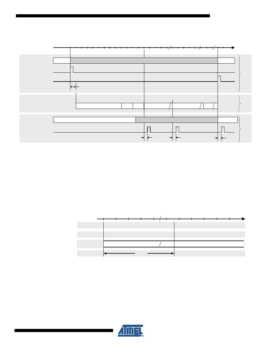
Figure 7-2.
Timing of RX_START, AMI and TRX_END Interrupts in Basic Operating Mode
7.1.4
Basic Operating Mode Timing
The following paragraphs depict state transitions and their timing properties. Timing figures are
explained in
Section 12.4 “Digital Interface Timing Characteristics” on
.
7.1.4.1
Power-on Procedure
The power-on procedure to P_ON state is shown in
.
Figure 7-3.
Power-on Procedure to P_ON State
When the external supply voltage (V
DD
) is firstly supplied to the AT86RF231, the radio trans-
ceiver enables the crystal oscillator (XOSC) and the internal 1.8V voltage regulator for the digital
domain (DVREG). After t
TR1
= 380 µs (typ.), the master clock signal is available at pin 17
(CLKM) at default rate of 1 MHz. If CLKM is available the SPI is already enabled and can be
used to control the transceiver. As long as no state change towards state TRX_OFF is per-
formed the radio transceiver remains in P_ON state.
128
160
192
0
192+(9+m)*32
-16
Time [µs]
RX
(Dev
ic
e 2)
IRQ_2 (RX_START)
RX_ON
RX_ON
IRQ
TRX_STATE
Interrupt latency
TRX_END
IRQ_5 (AMI)
t
IRQ
BUSY_RX
IRQ_3 (TRX_END)
TX
(D
e
v
ic
e1
)
PLL_ON
BUSY_TX
PLL_ON
IRQ
SLP_TR
TRX_STATE
Typ. Processing Delay
16 µs
Fr
am
e
on Ai
r
Preamble
SFD
PHR
MSDU
4
1
1
m
Number of Octets
Frame Content
MHR
7
FCS
2
t
IRQ
t
IRQ
0
Event
State
V
DD
on
P_ON
Block
XOSC, DVREG
100
CLKM on
400
Time [µs]
Time
t
TR1