Toshiba H1 SERIES TLCS-900 User Manual
Page 240
TMP92CM22
2007-02-16
92CM22-238
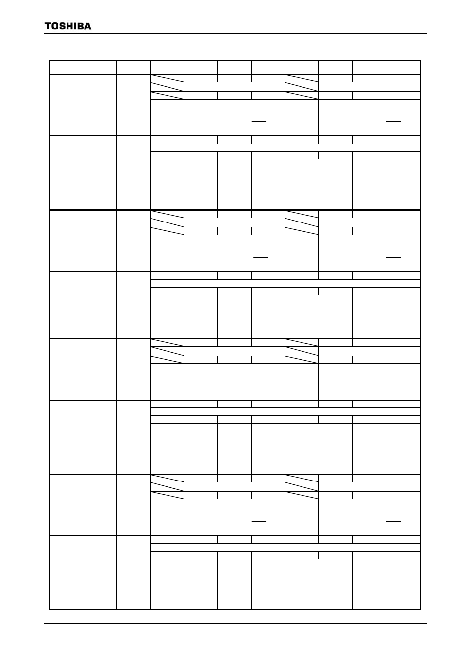
(4) Memory controller (1/2)
Symbol Name
Address
7 6 5 4 3 2 1 0
B0WW2
B0WW1
B0WW0
B0WR2
B0WR1
B0WR0
W W
0 1 0 0 1 0
B0CSL
Block 0
MEMC
control
register
low
0140H
(Prohibit
RMW)
Write
waits
001: 0 waits
010: 1 wait
101: 2 waits
110: 3 waits
111: 4 waits 011:
WAIT
pin
Others: Reserved
Read
waits
001: 0 waits
010: 1 wait
101: 2 waits
110: 3 waits
111: 4 waits 011:
WAIT
pin
Others: Reserved
B0E
−
− B0REC
B0OM1
B0OM0
B0BUS1
B0BUS0
W
0 0 0 0 0 0 0/1
0/1
B0CSH
Block 0
MEMCT
control
register
high
0141H
(Prohibit
RMW)
CS select
0: Disable
1: Enable
Always
write “0”.
Always
write “0”.
0: No insert
dummy
cycle
(Default)
1: Insert
dummy
cycle
00: ROM/SRAM
01: Reserved
10: Reserved
11: Reserved
Data bus width
00: 8 bits
01: 16 bits
10: Reserved
11: Reserved
B1WW2
B1WW1
B1WW0
B1WR2
B1WR1
B1WR0
W W
0 1 0 0 1 0
B1CSL
Block 1
MEMC
control
register
low
0144H
(Prohibit
RMW)
Write
waits
001: 0 waits
010: 1 wait
101: 2 waits
110: 3 waits
111: 4 waits 011:
WAIT
pin
Others: Reserved
Read
waits
001: 0 waits
010: 1 wait
101: 2 waits
110: 3 waits
111: 4 waits 011:
WAIT
pin
Others: Reserved
B1E
−
− B1REC
B1OM1
B1OM0
B1BUS1
B1BUS0
W
0 0 0 0 0 0 0/1
0/1
B1CSH
Block 1
MEMC
control
register
high
0145H
(Prohibit
RMW)
CS select
0: Disable
1: Enable
Always
write “0”.
Always
write “0”.
0: No insert
dummy
cycle
(Default)
1: Insert
dummy
00: ROM/SRAM
01: Reserved
10: Reserved
11: Reserved
Data bus width
00: 8
bits
01: 16
bits
10: Reserved
11: Reserved
B2WW2
B2WW1
B2WW0
B2WR2
B2WR1
B2WR0
W W
0 1 0 0 1 0
B2CSL
Block 2
MEMC
control
register
low
0148H
(Prohibit
RMW)
Write
waits
001: 0 waits
010: 1 wait
101: 2 waits
110: 3 waits
111: 4 waits 011:
WAIT
pin
Others: Reserved
Read
waits
001: 0 waits
010: 1 wait
101: 2 waits
110: 3 waits
111: 4 waits 011:
WAIT
pin
Others: Reserved
B2E B2M
− B2REC
B2OM1
B2OM0
B2BUS1
B2BUS0
W
1 0 0 0 0 0 0/1
0/1
B2CSH
Block 2
MEMC
control
register
high
0149H
(Prohibit
RMW)
CS select
0: Disable
1: Enable
0: 16 MB
1: Sets
area
Always
write “0”.
0: No insert
dummy
cycle
(Default)
1: Insert
dummy
cycle
00: ROM/SRAM
01: Reserved
10: Reserved
11: Reserved
Data bus width
00: 8 bits
01: 16 bits
10: Reserved
11: Reserved
B3WW2
B3WW1
B3WW0
B3WR2
B3WR1
B3WR0
W W
0 1 0 0 1 0
B3CSL
Block 3
MEMC
control
register
low
014CH
(Prohibit
RMW)
Write
waits
001: 0 waits
010: 1 wait
101: 2 waits
110: 3 waits
111: 4 waits 011:
WAIT
pin
Others: Reserved
Read
waits
001: 0 waits
010: 1 wait
101: 2 waits
110: 3 waits
111: 4 waits 011:
WAIT
pin
Others: Reserved
B3E
−
− B3REC
B3OM1
B3OM0
B3BUS1
B3BUS0
W
0 0 0 0 0 0 0/1
0/1
B3CSH
Block 3
MEMC
control
register
high
014DH
(Prohibit
RMW)
CS select
0: Disable
1: Enable
Always
write “0”.
Always
write “0”.
0: No insert
dummy
cycle
(Default)
1: Insert
dummy
cycle
00: ROM/SRAM
01: Reserved
10: Reserved
11: Reserved
Data bus width
00: 8 bits
01: 16 bits
10: Reserved
11: Reserved