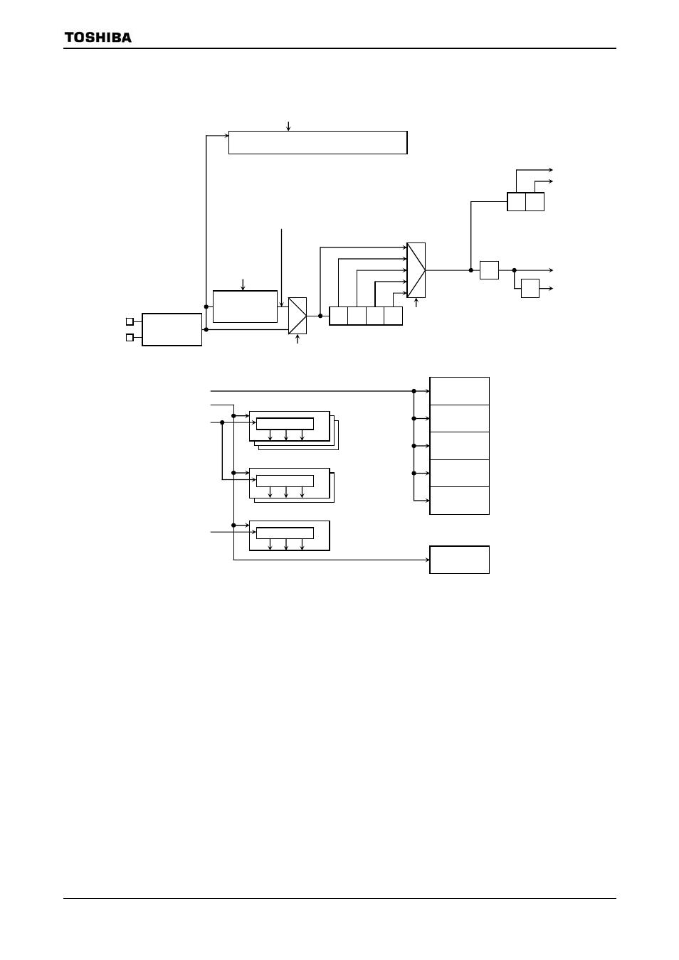
1 block diagram of system clock – Toshiba H1 SERIES TLCS-900 User Manual
Page 15

TMP92CM22
2007-02-16
92CM22-13
3.3.1
Block Diagram of System Clock
Figure 3.3.2 Block Diagram of Dual Clock and System Clock
ч4
ч16
ч8
ч4
ч2
X2
fc/16
fc/8
fc/4
fc/2
÷8
φT
φT0
f
FPH
ч2
ч2
f
SYS
f
iO
fc
PLLCR
Clock gear
High-
frequency
oscillator
X1
PLLCR
Warm-up timer (for high-frequency
oscillator)/lockup (for PLL) timer
SYSCR1
f
OSCH
SYSCR2
PLLCR
CPU
RAM
Interrupt
controller
ADC
I/O port
WDT
f
SYS
f
iO
Prescaler
SIO0 and SIO1
Prescaler
φT0
f
PLL
= f
OSCH
× 4
SBI
Prescaler
φT
TMRA0 to TMRA3 and
TMRB0 to TMRB1
PLL
(Clock doubler)
This manual is related to the following products:
See also other documents in the category Toshiba Hardware:
- MK4007GAL (9 pages)
- DVD-ROM DRIVE SD-M1712 (16 pages)
- OIS40R (2 pages)
- IVP8 (71 pages)
- MK8016GSG (2 pages)
- Tecra 061215 (38 pages)
- G9 ETB006Z (1 page)
- SD-R2412 (12 pages)
- OIS50 (2 pages)
- PCX1000 (18 pages)
- MK6026GAX (11 pages)
- Entone 95-810500-00 (14 pages)
- SD-R1002 (16 pages)
- 512E (1 page)
- T2N (272 pages)
- MK3004GAH (9 pages)
- AR-B1375 (69 pages)
- AUXILIARY CABINET 431B (64 pages)
- MK1016GAP (11 pages)
- MK1234 (4 pages)
- A305 (3 pages)
- 1.8-INCH HARD DISK DRIVE MK6006GAH (9 pages)
- MK3006GAL (153 pages)
- AF 512E (2 pages)
- MK8007GAH (9 pages)
- BCN002Z (16 pages)
- DRIVE MK6022GAX (11 pages)
- MK2003GAH (9 pages)
- MK6006GAH (157 pages)
- XM-6802B (15 pages)
- Parani UD100 (1 page)
- V.90 (102 pages)
- MK4025GAS (11 pages)
- MK5002MPL (9 pages)
- SD-R1512 (17 pages)
- Rockbox F Series (177 pages)
- (HDD2188) (11 pages)
- Low Voltage Motors VR Series (2 pages)
- MK1214GAP (11 pages)
- SD-M2012C (16 pages)
- 480082-D0 (9 pages)
- SD-C2712 (12 pages)
- HDD2188 MK8025GAS (11 pages)
- Electromagnetic Flowmeter Converter TIC-LF232A (8 pages)
- P000233790 (53 pages)
