5 serial channel timing (i/o interface mode) – Toshiba H1 SERIES TLCS-900 User Manual
Page 226
TMP92CM22
2007-02-16
92CM22-224
4.5
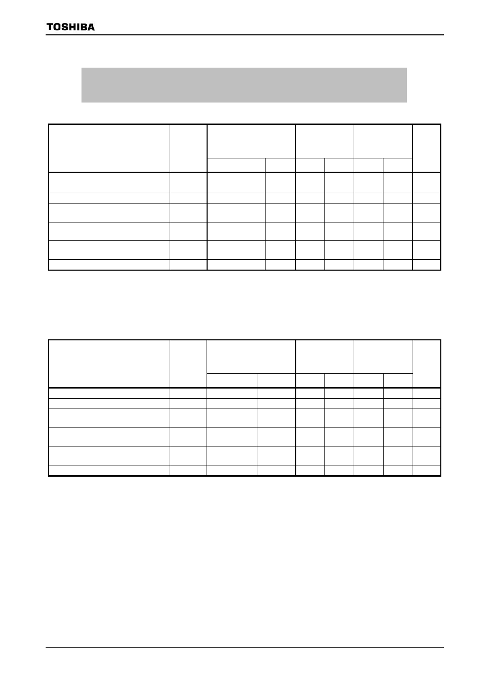
Serial Channel Timing (I/O interface mode)
Note: Symbol “X” in the following table means the period of clock “f
SYS
”, it’s same period of the system clock
“f
SYS
” for CPU core. The period of f
SYS
depends on the clock gear setting or changing high-speed
oscillator/low-speed oscillator and so on.
(1) SCLK
input
mode
Variable
f
SYS
=
20 MHz
(fc
= 40 MHz)
f
SYS
=
125 kHz
(fc
= 4 MHz)
Parameter Symbol
Min
Max
Min Max Min Max
Unit
SCLK period
t
SCY
16X
0.8
128
μs
Output data
→ SCLK rising/falling*
t
OSS
t
SCY
/2
− 4X − 110
90
31890
ns
SCLK
rising/falling*
→ Output data hold
t
OHS
t
SCY
/2
+ 2X + 0
500
80000
ns
SCLK
rising/falling*
→ Input data hold
t
HSR
3X
+ 10
160
24010
ns
SCLK
rising/falling
→ Valid data input
t
SRD
t
SCY
− 0
800
128000
ns
Valid data input
→ SCLK rising/falling
t
RDS
0
0 0 ns
*) SCLK rinsing/falling edge:
The rising edge is used in SCLK rising mode.
The falling edge is used in SCLK falling mode.
Note:
Value of f
SYS
= 20 MHz, 125 kHz is value if t
SCY
= 16X.
(2) SCLK output mode
Variable
f
SYS
=
20 MHz
(fc
= 40 MHz)
f
SYS
=
125 kHz
(fc
= 4 MHz)
Parameter Symbol
Min Max
Min
Max
Min
Max
Unit
SCLK period
t
SCY
16X
8192X
0.8
409.6
128
65536
μs
Output data
→ SCLK rising/falling*
t
OSS
t
SCY
/2
− 40 360
3960
ns
SCLK
rising/falling*
→ Output data hold t
OHS
t
SCY
/2
− 40 360
3960
ns
SCLK
rising/falling*
→ Input data hold
t
HSR
0
0
0
ns
SCLK
rising/falling
→ Valid data input
t
SRD
t
SCY
− 1X
− 180
409.4 65528
ns
Valid data input
→ SCLK rising/falling t
RDS
1X
+ 180
230
8180
ns