1 block diagram – Toshiba H1 SERIES TLCS-900 User Manual
Page 123
TMP92CM22
2007-02-16
92CM22-121
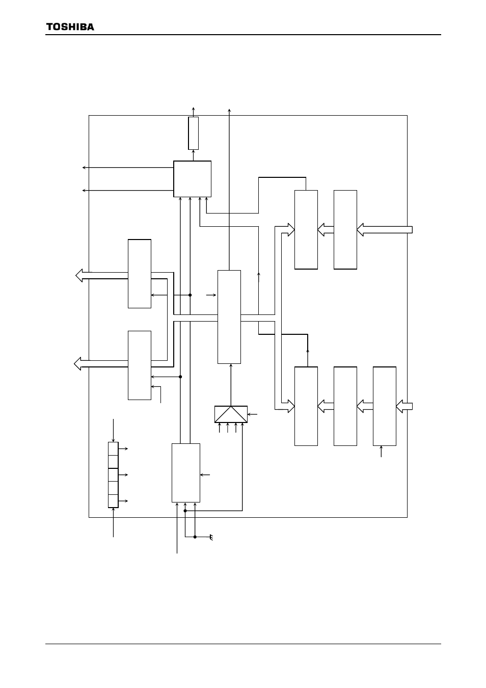
3.8.1 Block
Diagram
Figure 3.8.1 Block Diagram of TMRB0
Capture,
external interrupt
control
Ti
mer
flip-
flop
control
Match detection
Match
detection
32
16
8
4
2
φT1
φT4
φT16
Run/
clear
φT1
φT4
φT16
TB0MOD
Pr
escaler
clock:
φT0
Selecto
r
Register buffer
1
0
TB0RUN<
TB0R
UN>
TB0MOD
TB0FF
0
Internal data bus
TB0RUN
TB0RUN
Intenal data bus
TB0MO
D
Register 1
INTTB01
TB0OUT0
16-bit timer regis
ter
TB0REG0H/L
16-bit comparato
r
(CP10)
16-bit timer regis
ter
TB0R
G1H/L
16-bit comparato
r (CP11
)
TB0MO
D
Internal data bus
Internal data bus
Register 0
INTTB00
Ti
mer fl
ip
-fl
op
output
Ti
me
r
flip-
flop
Overflow
in
terrupt
INTTB
OF0
Capture register 0
TB0CP0H/L
Caputure registe
r
1
TB0CP1H/L
TA1O
UT
(from
TMRA01
)
16-bit up counter
(UC10
)
Count
clock
Interrup
t output