Toshiba H1 SERIES TLCS-900 User Manual
Page 117

TMP92CM22
2007-02-16
92CM22-115
In this mode, a programmable square wave is generated by inverting the timer output
each time the 8-bit up counter (UC0) matches the value in one of the timer registers
TA0REG or TA1REG.
The value set in TA0REG must be smaller than the value set in TA1REG.
Although the up counter for TMRA1 (UC1) is not used in this mode, TA01RUN
should be set to “1”, so that UC1 is set for counting.
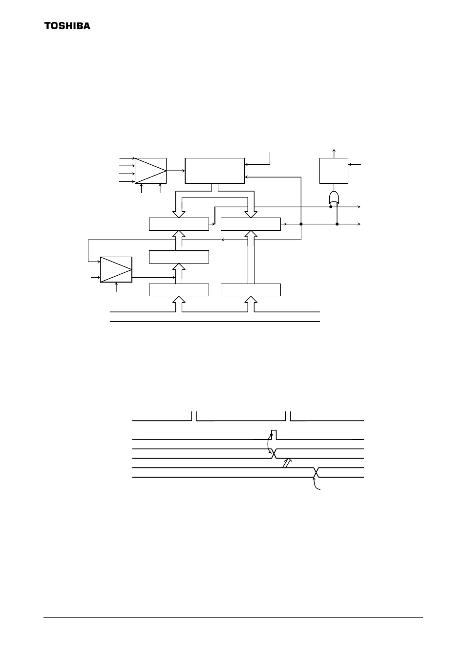
Figure 3.7.14 shows a block diagram representing this mode.
Figure 3.7.14 Block Diagram of 8-Bit PPG Output Mode
If the TA0REG double buffer is enabled in this mode, the value of the register buffer will
be shifted into TA0REG each time TA1REG matches UC0.
Use of the double buffer facilitates the handling of low-duty waves (when duty is varied).
Figure 3.7.15 Operation of Register Buffer
Q
2
Q
1
Match with TA0REG
and UC0
Match withTA1REG
Q
3
Q
2
(Up counter = Q
2
)
(Up counter = Q
2
)
Shift into register buffer
Write TA0REG (Register buffer)
TA0REG (Value of compare)
Register buffer
8-bit
up counter
(UC0)
Comparator
Comparator
TA0IN
φT1
φT4
φT16
TA01MOD
TA1FF
TA0REG
Register buffer
TA1REG
TA01RUN
TA0REG-WR
TA01RUN
TA1OUT
TA1FFCR
INTTA0
INTTA1
Shift trigger
Internal data bus
Selector
Inversion
Selector
