Toshiba H1 SERIES TLCS-900 User Manual
Page 152
TMP92CM22
2007-02-16
92CM22-150
(6) The receiving buffers
To prevent overrun errors, the receiving buffers are arranged in a double-buffer
structure.
Received data is stored one bit at a time in receiving buffer 1 (which is a shift
register). When 7 or 8 bits of data have been stored in receiving buffer 1, the stored
data is transferred to receiving buffer 2 (SC0BUF); this causes an INTRX0 interrupt to
be generated.
The CPU only reads receiving buffer 2 (SC0BUF). Even before the CPU reads
receiving buffer 2 (SC0BUF), the received data can be stored in receiving buffer 1.
However, unless receiving buffer 2 (SC0BUF) is read before all bits of the next data
are received by receiving buffer 1, an overrun error occurs. If an overrun error occurs,
the contents of receiving buffer 1 will be lost, although the contents of receiving buffer
2 and SC0CR
SC0CR
the most significant bit (MSB) – in 9-bit UART mode.
In 9-bit UART mode the wake-up function for the slave controller is enabled by
setting SC0MOD0
value of SC0CR
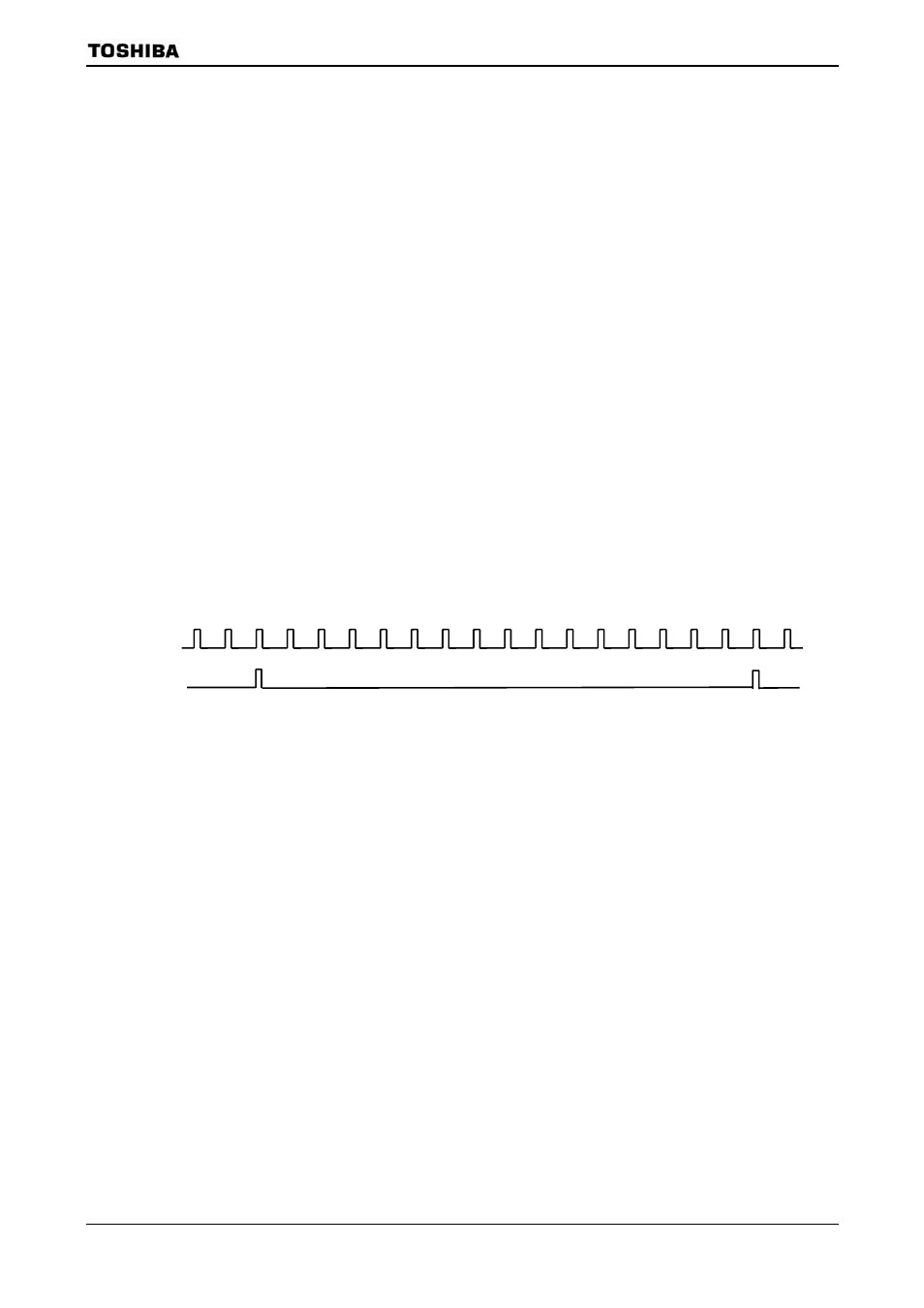
(7) Transmission counter
The transmission counter is a 4-bit binary counter that is used in UART mode and
which, like the receiving counter, counts the SIOCLK clock pulses; a TXDCLK pulse is
generated every 16 SIOCLK clock pulses.
Figure 3.9.4 Generation of Transmission Clock
(8) Transmission controller
• In I/O interface mode
In SCLK output mode with the setting SC0CR
= 0, the data in the
transmission buffer is output one bit at a time to the TXD0 pin on the rising or
falling edge of the shift clock which is output on the SCLK0 pin, according to the
SC0CR
In SCLK input mode with the setting SC0CR
= 1, the data in the
transmission buffer is output one bit at a time on the TXD0 pin on the rising or
falling edge of the SCLK0 input, according to the SC0CR
• In UART mode
When transmission data sent from the CPU is written to the transmission buffer,
transmission starts on the rising edge of the next TXDCLK, generating a
transmission shift clock TXDSFT.
15
16 1 2 3 4 5
6
7
8
9
10
11
12
13
14
15
16 1 2
SIOCLK
TXDCLK