5 power switch interface, 6 internal ring oscillator – Texas Instruments Dual/Single Socket CardBus and UntraMedia Controller PCI7621 User Manual
Page 64
3−8
3.5.5
Power Switch Interface
The power switch interface of the PCI7x21/PCI7x11 controller is a 3-pin serial interface. This 3-pin interface is
implemented such that the PCI7x21/PCI7x11 controller can connect to both the TPS2226 and TPS2228 power
switches. Bit 10 (12V_SW_SEL) in the general control register (PCI offset 86h, see Section 4.31) selects the power
switch that is implemented. The PCI7x21/PCI7x11 controller defaults to use the control logic for the TPS2228 power
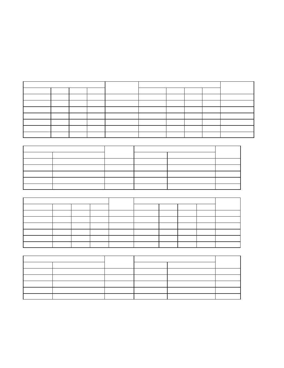
switch. See Table 3−3 and Table 3−6 below for the power switch control logic.
Table 3−3. TPS2228 Control Logic—xVPP/VCORE
AVPP/VCORE CONTROL SIGNALS
OUTPUT
V_AVPP/VCORE
BVPP/VCORE CONTROL SIGNALS
OUTPUT
V_BVPP/VCORE
D8(SHDN)
D0
D1
D9
OUTPUT
V_AVPP/VCORE
D8(SHDN)
D4
D5
D10
OUTPUT
V_BVPP/VCORE
1
0
0
X
0 V
1
0
0
X
0 V
1
0
1
0
3.3 V
1
0
1
0
3.3 V
1
0
1
1
5 V
1
0
1
1
5 V
1
1
0
X
Hi-Z
1
1
0
X
Hi-Z
1
1
1
0
Hi-Z
1
1
1
0
Hi-Z
1
1
1
1
1.8 V
1
1
1
1
1.8 V
0
X
X
X
Hi-Z
0
X
X
X
Hi-Z
Table 3−4. TPS2228 Control Logic—xVCC
AVCC CONTROL SIGNALS
OUTPUT
V_AVCC
BVCC CONTROL SIGNALS
OUTPUT
V_BVCC
D8(SHDN)
D3
D2
OUTPUT
V_AVCC
D8(SHDN)
D6
D7
OUTPUT
V_BVCC
1
0
0
0 V
1
0
0
0 V
1
0
1
3.3 V
1
0
1
3.3 V
1
1
0
5 V
1
1
0
5 V
1
1
1
0 V
1
1
1
0 V
0
X
X
Hi-Z
0
X
X
Hi-Z
Table 3−5. TPS2226 Control Logic—xVPP
AVPP CONTROL SIGNALS
OUTPUT
V_AVPP
BVPP CONTROL SIGNALS
OUTPUT
V_BVPP
D8(SHDN)
D0
D1
D9
OUTPUT
V_AVPP
D8(SHDN)
D4
D5
D10
OUTPUT
V_BVPP
1
0
0
X
0 V
1
0
0
X
0 V
1
0
1
0
3.3 V
1
0
1
0
3.3 V
1
0
1
1
5 V
1
0
1
1
5 V
1
1
0
X
12 V
1
1
0
X
12 V
1
1
1
X
Hi-Z
1
1
1
X
Hi-Z
0
X
X
X
Hi-Z
0
X
X
X
Hi-Z
Table 3−6. TPS2226 Control Logic—xVCC
AVCC CONTROL SIGNALS
OUTPUT
V_AVCC
BVCC CONTROL SIGNALS
OUTPUT
V_BVCC
D8(SHDN)
D3
D2
OUTPUT
V_AVCC
D8(SHDN)
D6
D7
OUTPUT
V_BVCC
1
0
0
0 V
1
0
0
0 V
1
0
1
3.3 V
1
0
1
3.3 V
1
1
0
5 V
1
1
0
5 V
1
1
1
0 V
1
1
1
0 V
0
X
X
Hi-Z
0
X
X
Hi-Z
3.5.6
Internal Ring Oscillator
The internal ring oscillator provides an internal clock source for the PCI7x21/PCI7x11 controller so that neither the
PCI clock nor an external clock is required in order for the PCI7x21/PCI7x11 controller to power down a socket or
interrogate a PC Card. This internal oscillator, operating nominally at 16 kHz, is always enabled.