2 suggested tfth and rfth for dma servicing, Sacr1) -10, Fifo write/read table -10 – Intel PXA255 User Manual
Page 496: Tfth and rfth values for dma servicing -10, Section 14.6.2, Section 14.6.1.2, Table 14-4, For deta, For det, 2 serial audio controller i
14-10
Intel® PXA255 Processor Developer’s Manual
Inter-Integrated-Circuit Sound (I2S) Controller
14.6.1.2
Suggested TFTH and RFTH for DMA servicing
The DMA controller can only be programmed to transfer 8, 16, or 32 bytes of data. This
corresponds to 2, 4, or 8 FIFO samples.
shows the recommended TFTH and RFTH
values to prevent Transmit FIFO over-run errors and Receive FIFO under-run errors.
14.6.2
Serial Audio Controller I
2
S/MSB-Justified Control Register
(SACR1)
SACR1, shown in
, specifically controls the I2S and MSB-Justified modes.
SACR1 bits DRPL, DREC, and AMSL cross clock domains. They are registered in an internal
clock domain that is much faster than the BITCLK domain. It takes 4 BITCLK cycles and 4
internal clock cycles before these controls are conveyed to the slower BITCLK domain. If the
above control settings are modified at a rate faster than (4 BITCLK + 4 internal clock) cycles, the
last updated value in this time frame is stored in a temporary register and is transferred to the
BITCLK domain.
This is a read/write register. Ignore reads from reserved bits. Write zeros to reserved bits.
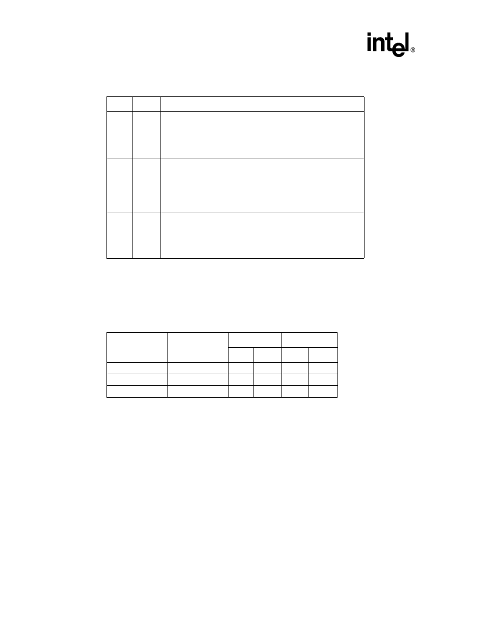
Table 14-4. FIFO Write/Read table
EFWR
STRF
Description
0
x
Normal CPU/DMA Write/Read condition:
•
A write access to the Data Register writes a Transmit FIFO entry.
•
A read access to the Data Register reads out a Receive FIFO entry.
•
I2SLINK reads from the Transmit FIFO and writes to the Receive
FIFO.
1
0
CPU or DMA only writes and reads Transmit FIFO:
•
A write access to the Data Register writes a Transmit FIFO entry.
•
A read access to the Data Register reads out a Transmit FIFO
entry.
•
I2SLINK cannot read the Transmit FIFO but can write to the
Receive FIFO.
1
1
CPU or DMA only writes and reads Receive FIFO:
•
A write access to the Data Register writes a Receive FIFO entry.
•
A read access to the Data Register reads out a Receive FIFO entry.
•
I2SLINK can read the Transmit FIFO but cannot write to the
Receive FIFO.
Table 14-5. TFTH and RFTH Values for DMA Servicing
DMA Transfer Size
# of FIFO entries
TFTH Value
RFTH Value
Min
Max
Min
Max
8 Bytes
2
0
14
1
15
16 Bytes
4
0
12
3
15
32 Bytes
8
0
8
7
15