4 external logic for 16-bit pc card implementation, Bit i/o space write commands (niois16 = 1) -64, Bit i/o space read commands (niois16 = 1) -64 – Intel PXA255 User Manual
Page 246: Table 6-35
6-64
Intel® PXA255 Processor Developer’s Manual
Memory Controller
6.8.4
External Logic for 16-Bit PC Card Implementation
The PXA255 processor requires external glue logic to complete the 16-bit PC Card socket interface
that allows either 1-socket or 2-socket solutions.
and
show general solutions for a one- and two-socket configuration. The
pull-ups shown are included as specified in the PC Card Standard - Volume 2 - Electrical
Specification. Low-power systems must remove power from the pull-ups during sleep to avoid
unnecessary power consumption.
GPIO or memory-mapped external registers can be used to control the reset of the 16-bit PC Card
interface, power selection (V
CC
and V
PP
), and drive enables. The INPACK# signal is not used.
and
provide the logical connections necessary to support hot insertion
capability. For dual-voltage support, level shifting buffers are required for all PXA255 processor
input signals. Hot insertion capability requires that each socket be electrically isolated from the
other and from the remainder of the memory system. If one or both of these features is not required,
then some of the logic shown in the following diagrams can be eliminated.
Software is responsible for setting the MECR[NOS] and MECR[CIT] bits. NOS indicates the
number of sockets that the system support while CIT is written when the Card is in place. Input
pins nPWAIT and nIOIS16 are three stated until card detect (CD) signal is asserted. To achieve
this, software programs the MECR[CIT] bit when a card is detected. If the MECR[CIT] is 0, the
nPWAIT and nIOIS16 inputs are ignored.
shows the minimal glue logic needed for a 1-socket system, including: data
transceivers, address buffers, and level shifting buffers. The transceivers are enabled by the
PSKTSEL signal. The DIR pin of the transceiver is driven by the RD/nWR pin. A GPIO is used for
the three-state signal of the address and nPWE lines. These signals must be three-stated because
they are used for memories other than the card interface. The Card Detect[1:0] signals are driven
by the signal device.
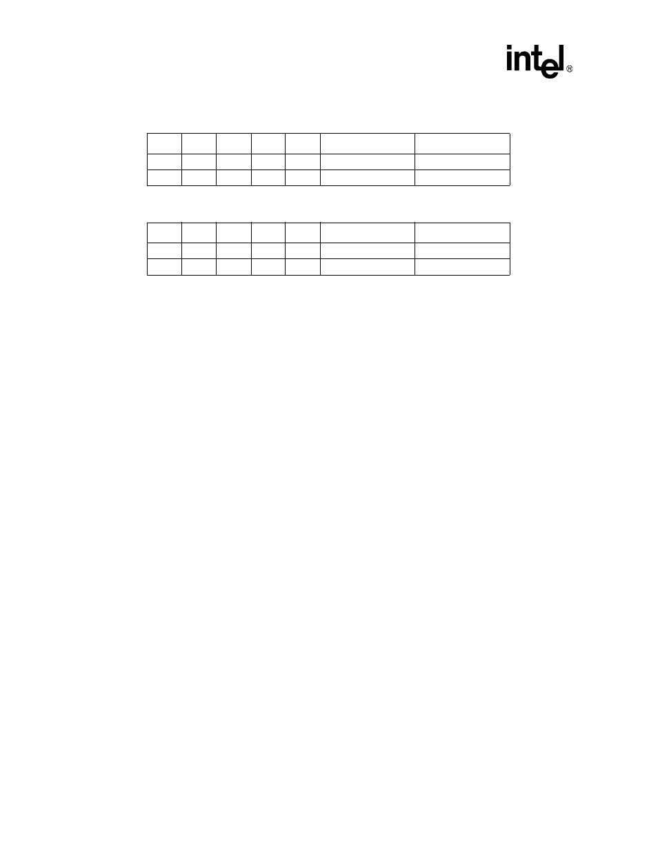
Table 6-34. 8-Bit I/O Space Write Commands (nIOIS16 = 1)
nPCE2 nPCE1 MA<0> nPIOR nPIOW
MD[15:8]
MD[7:0]
1
0
0
1
0
Unimportant
Even Byte
1
0
1
1
0
Unimportant
Odd Byte
Table 6-35. 8-Bit I/O Space Read Commands (nIOIS16 = 1)
nPCE2 nPCE1 MA<0> nPIOR nPIOW
MD[15:8]
MD[7:0]
1
0
0
0
1
Unimportant
Even Byte
1
0
1
0
1
Unimportant
Odd Byte