1 reset, 2 internal register descriptions, Example nrz bit encoding – (0b0100 1011 -5 – Intel PXA255 User Manual
Page 361

Intel® PXA255 Processor Developer’s Manual
10-5
UARTs
or if odd parity is enabled and the data byte has an even number of ones. The data frame ends with
one, one and a half or two stop bits, as programmed by software. The stop bits are represented by
one, one and a half, or two successive bit periods of a logic one.
Each UART has two FIFOs: one transmit and one receive. The transmit FIFO is 64 bytes deep and
eight bits wide. The receive FIFO is 64 bytes deep and 11 bits wide. Three bits are used for tracking
errors.
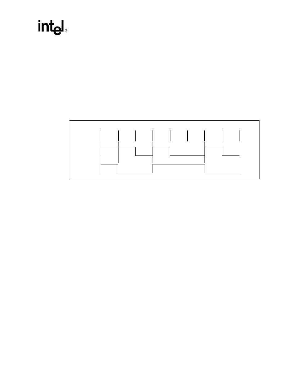
The UART can use NRZ coding to represent individual bit values. NRZ coding is enabled when the
Interrupt Enable Register’s (IER) bit 5, IER[5] is set to high. A one is represented by a line
transition and a zero is represented by no line transition.
1011 in NRZ coding. The byte’s LSB is transmitted first.
)
E
10.4.1
Reset
The UARTs are disabled on reset. To enable a UART, Software must program the GPIO registers
(see
Section 4.1, “General-Purpose I/O” on page 4-1
) then set IER[UUE]. When the UART is
enabled, the receiver waits for a frame start bit and the transmitter sends data if it is available in the
Transmit Holding Register. Transmit data can be written to the Transmit Holding Register before
the UART unit is enabled. In FIFO mode, data is transmitted from the FIFO to the Transmit
Holding Register before it goes to the pin.
When the UART unit is disabled, the transmitter or receiver finishes the current byte and stops
transmitting or receiving more data. Data in the FIFO is not cleared and transmission resumes
when the UART is enabled.
10.4.2
Internal Register Descriptions
Each UART has 13 registers: 12 registers for UART operation and one register for slow infrared
configuration. The registers are all 32-bit registers but only the lower eight bits have valid data.
The 12 UART operation registers share nine address locations in the I/O address space.
shows the registers and their addresses as offsets of a base address. The base address for each
UART is 32 bits. The state of the SLCR[DLAB] bit affects the selection of some UART registers.
To access the Baud Rate Generator Divisor Latch registers, software must set the SLCR[DLAB] bit
high.
Figure 10-2. Example NRZ Bit Encoding – (0b0100 1011
Digital
Data
NRZ
Data
Bit
Value
1
1
0
1
0
0
1
0
LSB
MSB
