7 lcd controller register summary, Lcd controller register summary -44, Tcr bit definitions -44 – Intel PXA255 User Manual
Page 306: Table 7-15, N in
7-44
Intel® PXA255 Processor Developer’s Manual
LCD Controller
7.7
LCD Controller Register Summary
shows the registers associated with the LCD Controller and the physical addresses used
to access them. All of the LCD registers must be accessed as 32-bit values.
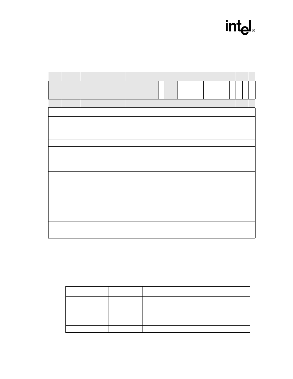
Table 7-15. TCR Bit Definitions
Physical Address
0X4400_0044
TMED Control Register
LCD Controller
Bit
31 30 29 28 27 26 25 24 23 22 21 20 19 18 17 16 15 14 13 12 11 10 9
8
7
6
5
4
3
2
1
0
reserved
TED
re
s
e
rv
e
d
THBS
TVBS
FN
A
M
E
CO
AE
FN
A
M
CO
A
M
Reset
X
X
X
X
X
X
X
X
X
X
X
X
X
X
X
X
X
1
1
1
0
1
0
1
0
1
0
0
1
1
1
1
Bits
Name
Description
31:15
—
reserved
14
TED
TMED Energy Distribution Matrix Select
0 = Selects Matrix 1
1 = Selects Matrix 2
13:12
—
reserved
11:8
THBS
TMED Horizontal Beat Suppression
Specifies the column shift value.
7:4
TVBS
TMED Vertical Beat Suppression
Specifies the block shift value.
3
FNAME
TMED Frame Number Adjuster Enable
0 = Disable frame number adjuster.
1 = Enable frame number adjuster.
2
COAE
TMED Color Offset Adjuster Enable
0 = Disable color offset adjuster.
1 = Enable color offset adjuster.
1
FNAM
TMED Frame Number Adjuster Matrix
0 = Selects Matrix 1 for frame number adjuster.
1 = Selects Matrix 2 for frame number adjuster.
0
COAM
TMED Color Offset Adjuster Matrix
0 = Selects Matrix 1 for color offset adjuster.
1 = Selects Matrix 2 for color offset adjuster.
Table 7-16. LCD Controller Register Summary (Sheet 1 of 2)
Address
Name
Description
0x4400_0000
LCCR0
LCD controller control register 0
0x4400_0004
LCCR1
LCD controller control register 1
0x4400_0008
LCCR2
LCD controller control register 2
0x4400_000C
LCCR3
LCD controller control register 3
0x4400_0020
FBR0
DMA channel 0 frame branch register