Epson Power Supply S1F70000 User Manual
Page 91
S1F76640 Series
2–48
EPSON
S1F70000 Series
Technical Manual
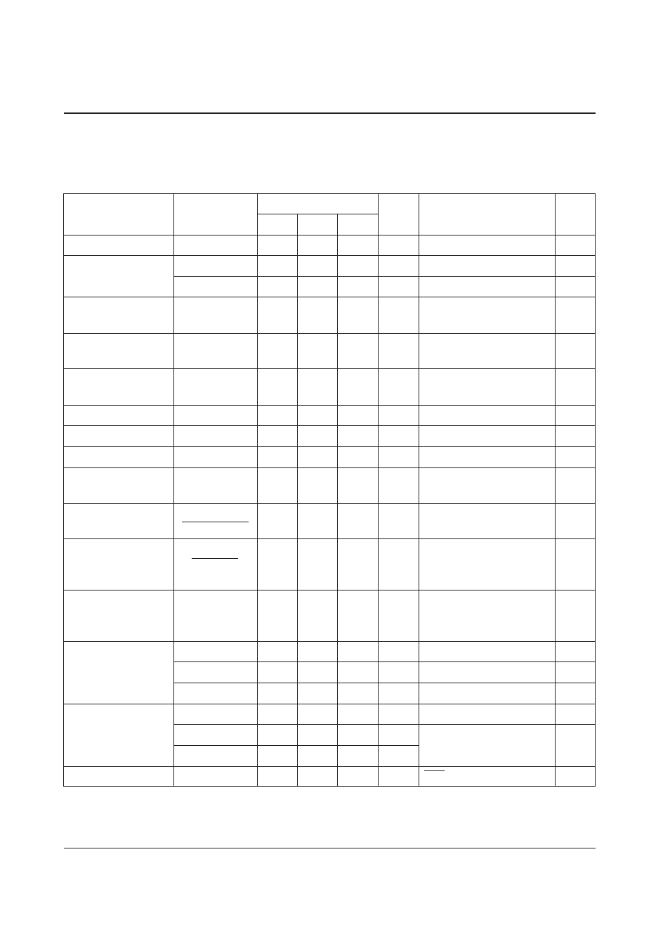
Electrical Characteristics
Unless otherwise specified, Ta=–40˚C to +85˚C
GND=0V, V
DD
=5V
Parameter
Symbol
Specification Value
Unit
Conditions
Measurement
Min.
Typ.
Max.
Circuit
Input supply voltage
V
DD
1.8
—
5.5
V
—
—
Output voltage
V
O
—
—
22
V
—
—
V
REG
V
RV
—
22
V
R=
∞
, R
RV
=1M
Ω
, V
O
=22V
2
Stabilization circuit
V
O
V
RV
+2.1
—
22
V
—
—
operating voltage
Step-up circuit current
I
OPR1
—
60
100
µ
A
R
L
=
∞
, R
OSC
=1M
Ω
1
consumption (V
DD
system)
Step-up circuit current
I
OPR2
—
12
25
µ
A
R
L
=
∞
, R
OSC
=1M
Ω
,
2
consumption (VRI system)
V
O
=20V
Static current
I Q
—
—
2
µ
A
TC2=TC1=V
O
,RI=
∞
1
Oscillation frequency
f
OSC
16
20
24
kHz
R
OSC
=1M
Ω
1
Output impedance
R
O
—
250
350
Ω
I
O
=10mA
1
Step-up power conversion
Peff
90
95
—
%
I
O
=5mA
1
efficiency (Note 2)
Stabilized output
∆
V
REG
—
0.2
—
%/V
10V O <20V,V REG =10V 2 voltage fluctuation ∆ V O ⋅ V REG R L = ∞ , Ta=25˚C Stabilized output load ∆ V REG — 5.0 — Ω V O =20V,V REG =15V 2 fluctuation (Note 3) ∆ I O Ta=25˚C,0 O <10mA TC1=V O ,TC2=GND Stabilized output saturation R SAT — 12 — Ω R SAT = ∆ (V O -V REG )/ ∆ I O 2 resistance (Note 4) 0 O <10mA,RV=V O Ta=25˚C Reference voltage V RV0 2.20 3.00 3.80 V TC2=GND,TC1=V O ,Ta=25˚C 2 V RV1 2.30 2.80 3.30 V TC2=TC1=GND,Ta=25˚C V RV2 1.70 2.00 2.30 V TC2=V O ,TC1=GND,Ta=25˚C Temperature gradient C T0 –0.45 –0.27 –0.10 %/˚C V DD =5V,V O =20V 2 C T1 –0.60 –0.42 –0.25 %/˚C (Note 5) C T2 –0.70 –0.55 –0.40 %/˚C Input leak current I LKI — — 2 µ A P OFF ,TC1,TC2,OSC1,RV pins 3