Epson – Epson Power Supply S1F70000 User Manual
Page 77
S1F76540 Series
2–34
EPSON
S1F70000 Series
Technical Manual
◊
Setup conditions of Figure 2.12
• Internal clock : ON (Low Output mode)
• Booster circuit : ON
• Regulator
: ON (if C
T
= –0.04%/
°
C)
◊
Power-off procedure
• Set the P
OFF1
pin to low (V
I
) to turn off all circuits.
◊
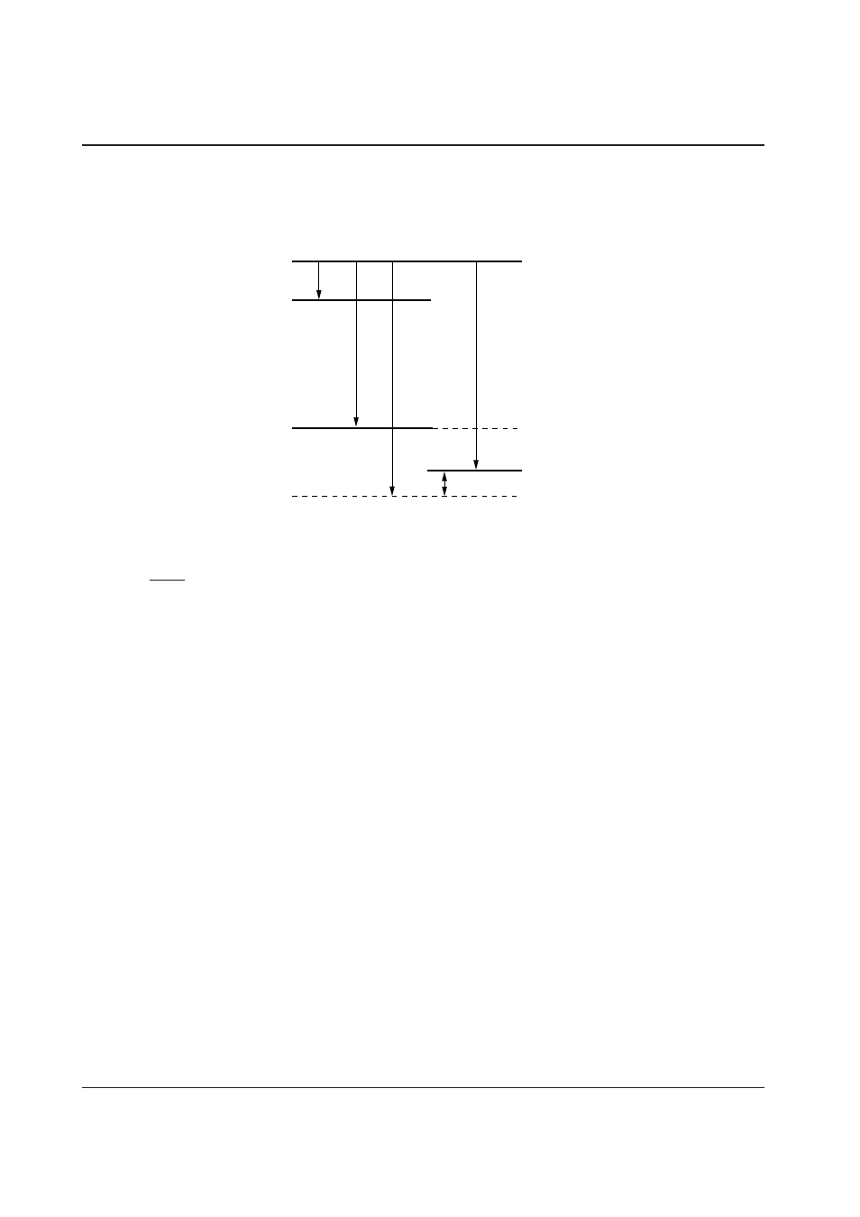
Output voltages
• When diodes are used for voltage boosting, the characteristics of diodes directly affect on the voltage boosting
characteristics. The forward voltage drop (V
F
) of diodes can reduce the booster output voltage. As the example
of Figure 2.12 uses two diodes, the drop of “V
F
” voltage multiplied by two occurs as shown in Figure 2.13. The
booster output voltage is expressed by equation (5).
To increase the |V
O
'| value, use the diodes having a smaller V
F
.
| V
O
' | = 6
×
| V
I
| – 2
×
V
F
• • • • Equation (5)
◊
Notes
1 Input and output current conditions
To satisfy the input and output current ratings, limit the total current does not exceed the rated input current.
The total current means the total boost time multiplied by the output load current. The example of Figure 2.12
has the maximum load current of 13.3 mA ( = 80 mA divided by 6).
2 Input and output voltage conditions
To satisfy the input and output voltage ratings, take care not to violate the electric potential relationship of
higher time boosting using diodes. The example of Figure 2.12 must have the “V
I
” that can satisfy the input
voltage conditions during 6-time boosting (see Table 2.3).
◊
Application in other setup conditions
1 When used in the High Output mode
Connect the FC pin to the V
I
pin.
2 When changing the temperature coefficient (C
T
)
Change the TC1 and TC2 pin setup by following the definition of Table 2.7.
V
DD
V
I
V
I
4V
I
6V
I
6V
I
– (2
∗
V
F
)
V
O
'
2
∗
V
F
V
O
Figure 2.13 Potential relationship during 6-time boosting using diodes