Epson, Larger time boosting using diodes – Epson Power Supply S1F70000 User Manual
Page 76
S1F76540 Series
S1F70000 Series
EPSON
2–33
Technical Manual
S1F76540
Series
◊
Setup conditions of Figure 2.11
First stage
Second stage
• Internal clock : ON (Low Output mode)
• Internal clock : OFF
• Booster circuit : ON
• Booster circuit : ON
• Regulator
: OFF
• Regulator
: ON (if C
T
= –0.04%/
°
C)
◊
Power-off procedure
• In Figure 2.11, when the P
OFF2
pin of the first-stage S1F76540 is set to low (V
I
), voltage boosting is stopped at
the first and second stages. However, the regulator at the second stage does not stop. Therefore, the voltage that
is approximately V
I
appears at V
REG
pin during |V
REG
| > |V
I
| setup.
• To set the V
REG
pin to high-impedance state, set both P
OFF1
and P
OFF2
pins to low at the first and second stages.
◊
Application in other setup conditions
1 When used in the High Output mode
• Connect the FC pin of the first-stage S1F76540 to the V
I
pin.
2 When changing the temperature coefficient (C
T
)
• Change the TC1 and TC2 pin setup by following the definition of Table 2.7.
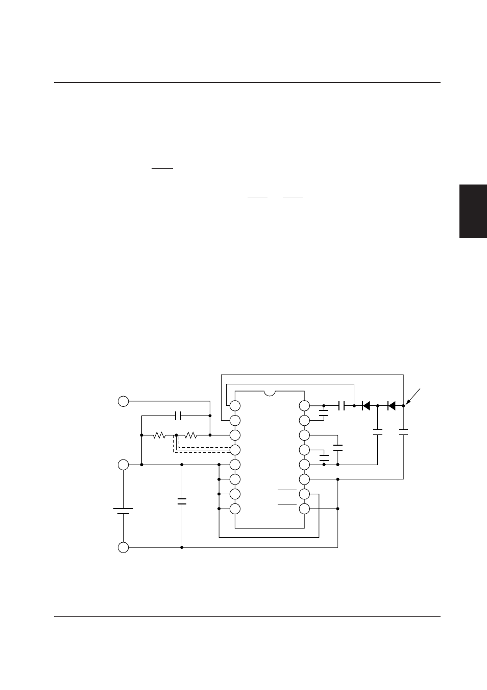
Larger Time Boosting Using Diodes
The S1F76540 can be configured to have the five-time
or larger voltage boosting and regulation by adding ex-
ternal diodes. As the booster output impedance in-
creases due to the diode forward voltage drop (V
F
), the
diodes having a smaller V
F
are recommended to use.
Figure 2.12 gives a wiring example of 6-time booster
and regulator that use two diodes. The wiring between
V
O
and V
RI
must be minimal. Figure 2.13 provides the
potential relationship.
Figure 2.12 Wiring example for 6-time boosting using diodes
+
+
C2
C4
+
+
+
+
C3
C5
D2
D1
C
O
V
O
'
C1
1
2
3
4
5
6
7
8
V
O
V
RI
V
REG
RV
V
DD
FC
TC1
TC2
C2P
C2N
C3N
C1N
C1P
V
I
P
OFF1
P
OFF2
16
15
14
13
12
11
10
9
+
R2
C
REG
R1
+
C
I
V
I
V
DD
V
REG