Pin descriptions – Epson Power Supply S1F70000 User Manual
Page 84
S1F76640 Series
S1F70000 Series
EPSON
2–41
Technical Manual
S1F76640
Series
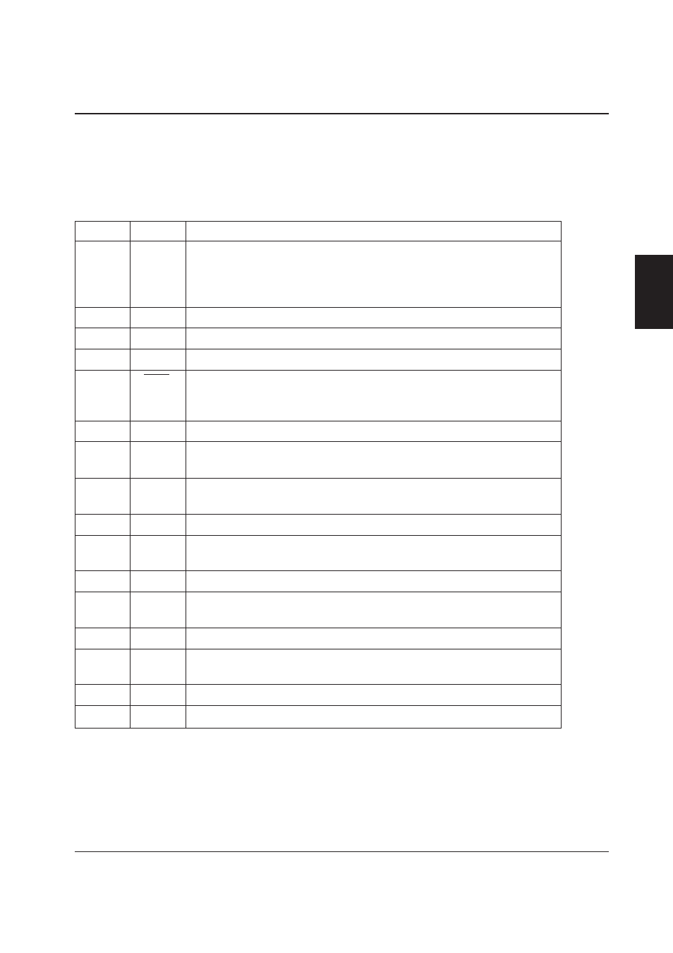
Pin No. Pin name
Description
1
RV
Stabilization voltage regulation pin.
When the intermediate tap of the external volume (3-pin resistor)
connected between the V
DD
pin and the V
REG
pin is connected to the
RV pin, V
REG
output voltage can be adjusted.
2
V
REG
Stabilized voltage output pin
3
TC1
Temperature gradient selection pin
4
TC2
Temperature gradient selection pin
5
P
OFF
V
REG
output ON/OFF control pin.
When control signal from the system side is input to this pin, the power
off (V
REG
output power off) control of S1F76640 becomes available.
6
GND
Power supply pin (minus side, system GND)
7
OSC1
Oscillation resistor connection pin.
This pin becomes the clock input pin when an external clock operates.
8
OSC2
Oscillation resistor connection pin.
This pin is released when an external clock operates.
9
V
DD
Power supply pin (plus side, system V
CC
)
10
CAP1–
Pump up capacitor minus side connection pin for 2 times step-up.
Next stage clock at series connection time.
11
CAP1+
Pump up capacitor plus side connection pin for 2 times step-up
12
CAP2–
Pump up capacitor minus side connection pin for 3 times step-up.
Output pin at 2 time step-up time (to be short-circuited to V
O
).
13
CAP2+
Pump up capacitor plus side connection pin for 3 times step-up
14
CAP3+
Pump up capacitor plus side connection pin for 4 times step-up.
Output pin at 3 times step-up time (to be short-circuited to V
O
).
15
V
O
Output pin at 3 times step-up time
16
V
RI
Stabilization circuit input pin
PIN DESCRIPTIONS