Epson, And r, The circuit must also satisfy the condition i – Epson Power Supply S1F70000 User Manual
Page 178
S1F76300 Series
S1F70000 Series
EPSON
4–33
Technical Manual
S1F76300
Series
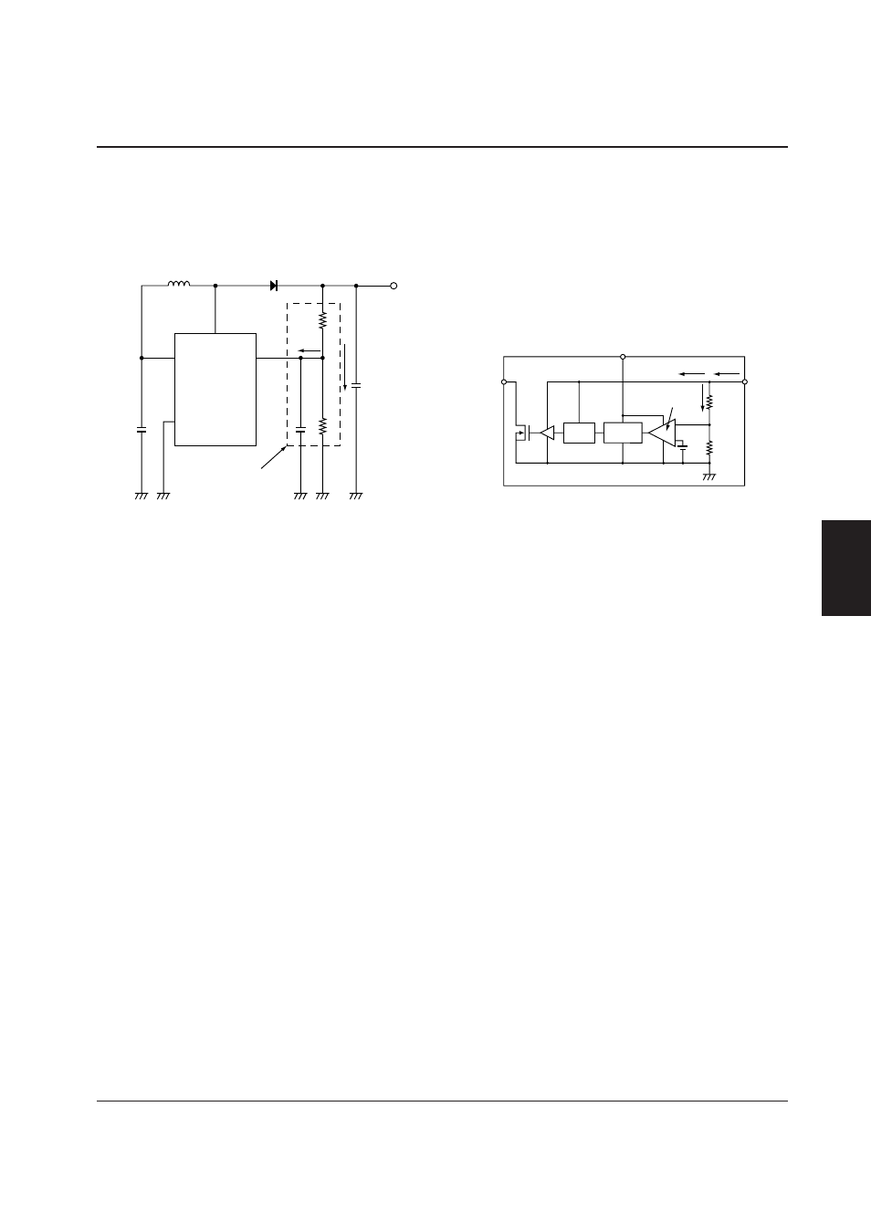
Output voltage adjustment
To ensure stable output, any circuit that adjusts the out-
put voltage must contain C1, R
A
and R
B
. To stop
switching current from affecting V
O
, the circuit must
also satisfy the condition I
O
< I
R
.
The following figure summarizes the relevant circuits
inside an S1F70000 series chip.
V
O
is connected to the level shift and buffer circuit,
which provide the gate bias for the switching transistor
driving the inductor. The current drain I
O1
, varies with
the load and is typically 10
µ
A. The current, I
O2
,
through the internal resistors R1 and R2 is typically
1
µ
A.
V
I
V
O
I
O
C
L
(I
O
< I
R
)
I
R
R
B
R
A
C
GND
V
SW
Voltage adjustment
circuit
Step-up
voltage
output
SCI7631M/C
V
SW
V
I
Comparator
Controller
Level
shifter
V
O
I
O1
I
O2
V
REF
R1
R2
I
O
Buffer