Pin assignments, Pin descriptions, Epson – Epson Power Supply S1F70000 User Manual
Page 45
S1F76610 Series
2–2
EPSON
S1F70000 Series
Technical Manual
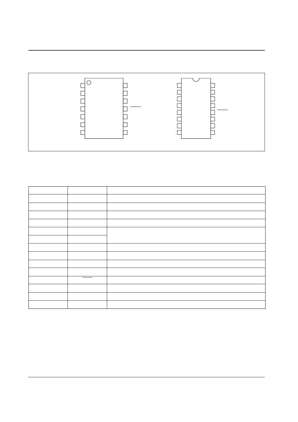
PIN ASSIGNMENTS
PIN DESCRIPTIONS
S1F76610C0B0/M0B0
1
2
3
4
5
6
7
8
1
2
3
4
5
6
7
CAP+
CAP–
CAP2+
CAP2–
TC1
TC2
V
I
14
13
12
11
10
9
8
V
DD
OSC1
OSC2
P
OFF
RV
V
REG
V
O
CAP+
CAP–
NC
CAP2+
CAP2–
TC1
TC2
V
I
V
DD
OSC1
NC
OSC2
P
OFF
RV
V
REG
V
O
16
15
14
13
12
11
10
9
S1F76610M2B0
S1F76610C0B0/M0B0
Description
Positive charge-pump connection for
×
2 multiplier
Negative charge-pump connection for
×
2 multiplier
Positive charge-pump connection for
×
3 multiplier
Negative charge-pump connection for
×
3 multiplier or
×
2 multiplier output
Pin No.
1
2
3
4
5
6
7
8
9
10
11
12
13
14
Pin name
CAP1+
CAP1–
CAP2+
CAP2–
TC1
TC2
V
I
V
O
V
REG
R
V
P
OFF
OSC2
OSC1
V
DD
Temperature gradient selects
Negative supply (system ground)
×
3 multiplier output
Voltage regulator output
Voltage regulator output adjust
Voltage regulator output ON/OFF control
Resistor connection. Open when using external clock
Resistor connection. Clock input when using external clock
Positive supply (system V
CC
)