Epson, Serial connection, Positive voltage conversion – Epson Power Supply S1F70000 User Manual
Page 56: Or other potential of the second stage v, Or up) and the second stage v, Off by p, Signals, if current flows into the second stage v, At the v, And v, Or up may not be applied to the v
S1F76610 Series
S1F70000 Series
EPSON
2–13
Technical Manual
S1F76610
Series
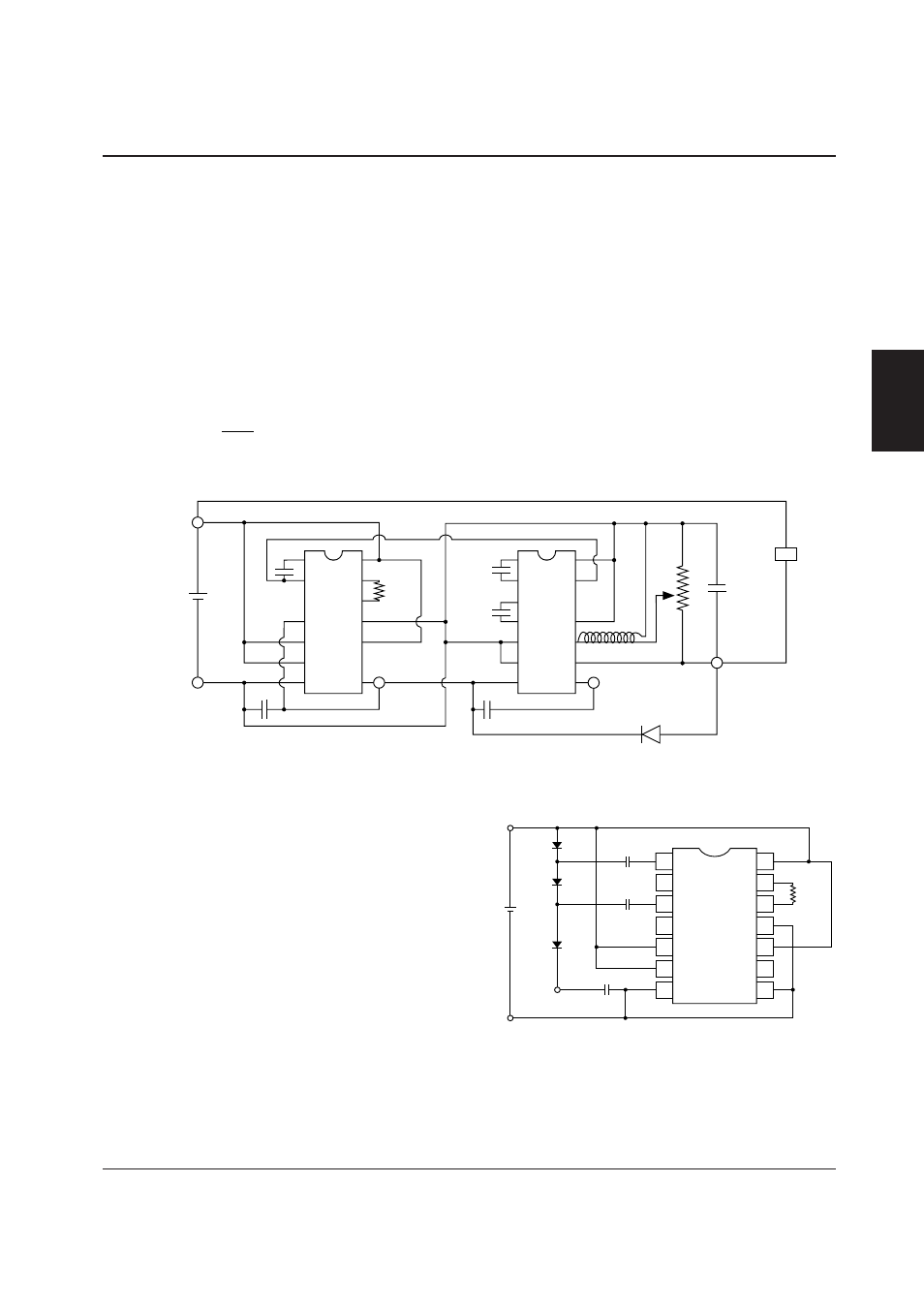
Serial Connection
Connecting two or more chips in series obtains a higher
output voltage than can be obtained using a parallel
In case of series connections, when connecting loads
between the first stage V
DD
(or other potential of the
second stage V
DD
or up) and the second stage V
REG
as
shown in Fig. 2-13, be cautions about the following
point.
* When normal output is not occurring at the V
REG
ter-
minal such as at times of starting up or when turning
the V
REG
off by P
OFF
signals, if current flows into the
second stage V
REG
terminal through the load from
connection, however, this also raises the output imped-
ance.
the first stage V
DD
(or other potential of the second
stage V
DD
or up) to cause a voltage exceeding the
absolute maximum rating for the second stage V
DD
at
the V
REG
terminal, normal operation of the IC may be
hampered. Consequently, When making a series
connection, insert a diode D1 between the second
stage V
I
and V
REG
as shown in Fig. 2-13 so that a
voltage exceeding the second stage V
DD
or up may
not be applied to the V
REG
terminal.
Positive Voltage Conversion
Adding diodes converts a negative voltage to a positive
one.
To convert the voltage tripler shown earlier to a voltage
doubler, remove C2 and D2, and short circuit D3. Small
Schottky diodes are recommended for all these diodes.
The resulting voltage is lowered by V
F
, the voltage drop
in the forward direction for each diode used. For ex-
ample, if V
DD
= 0V, V
I
= –5V, and V
F
= 0.6V, the re-
sulting voltages would be as follows.
• For a voltage tripler,
V
O
= 10 – (3
×
0.6) = 8.2V
• For a voltage doubler,
V
O
= 5 – (2
×
0.6) = 3.8V
10
µ
F
1M
Ω
10
µ
F
10
µ
F
+
–
+
–
V
DD
= 0V
V
O
= –20V
V
REG
'
= –15V
V
DD
'
= V
I
= –5V
D1
V
I
= –5V
5V
+
–
10
µ
F
+
–
+
1
2
3
4
5
6
7
14
13
12
11
10
9
8
1
2
3
4
5
6
7
14
13
12
11
10
9
8
10
µ
F
+
–
10
µ
F
100k
Ω
1M
Ω
to
–
Load
V
O
= –10V= V
I
V
I
= –5 V
V
DD
= 0 V
V
O
= 8.2 V
C3
10
µ
F
+
C2
10
µ
F
+
C1
10
µ
F
+
R
OSC
1 M
Ω
D1
D2
5 V
D3
1
2
3
4
5
6
7
14
13
12
11
10
9
8