Epson Power Supply S1F70000 User Manual
Page 68
S1F76540 Series
S1F70000 Series
EPSON
2–25
Technical Manual
S1F76540
Series
Reference Voltage Circuit
The S1F76540 has a built-in reference voltage circuit
for voltage regulation. The regulated voltage (ex-
plained in the next “voltage regulator circuit” section) is
set depending on the division ratio between this refer-
ence voltage and the external resistance. The reference
voltage can be used to change the temperature coeffi-
cient at pins TC1 and TC2. One of four states can be
selected as listed on Table 2.6.
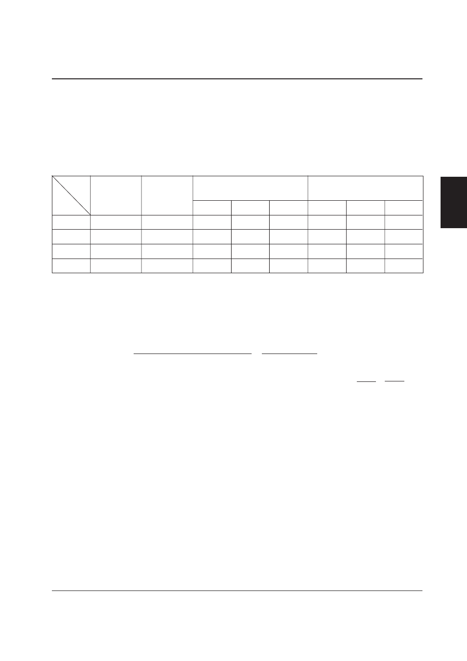
Table 2.6 Setup of reference voltage and temperature coefficient
TC1
TC2
Reference voltage,
Temperature coefficient,
(High = V
DD
) (High = V
DD
)
V
REF
(V)
C
T
(%/
°
C)
Mode
(Low = V
I
)
(Low = V
I
)
Min.
Typ.
Max.
Min.
Typ.
Max.
C
T0
High
High
–1.55
–1.5
–1.45
–0.07
–0.04
0
C
T1
High
Low
–1.70
–1.5
–1.30
–0.25
–0.15
–0.07
C
T2
Low
High
–1.90
–1.5
–1.10
–0.45
–0.35
–0.20
C
T3
Low
Low
–2.15
–1.5
–0.85
–0.75
–0.55
–0.30
Notes: 1. The reference voltage is given at Ta = 25
°
C.
2. The reference voltage and temperature coefficient of the chip products may vary depending
on the moldings used on each chip. Use these chips only after the temperature test.
The temperature coefficient (C
T
) is defined by the following equation. The negative sign of the temperature coeffi-
cient (C
T
) means that the |V
REF
| value decreases when the temperature rises.
C
T
=
| V
REF
(50
°
C) | – | V
REF
(0
°
C) |
×
100
50
°
C – 0
°
C
| V
REF
(25
°
C) |
Notes on TC1 and TC2 pin replacement:
• When replacing the TC1 and TC2 pins after power-on, always select the power-off mode (P
OFF1
= P
OFF2
= V
I
)
and replace them by each other.
Voltage Regulator Circuit
The voltage regulator circuit regulates a voltage entered
in the V
RI
pin and can output any voltage. It uses the
series voltage regulation. As shown in Figure 2.5, the
V
RI
and V
O
pins must be short-circuited by a jumper as
short as possible except for larger time boosting by us-
ing external diodes.
As shown by equation (1), any output voltage can be set
by the ratio of external division resistors R1 and R2.
The sum of division resistance is recommended to be
small as possible to avoid an external noise interfer-
ence. As the current consumed by division resistors
(equation (2)) flows, the 100
Ω
to 1M
Ω
are recom-
mended to use.
The temperature coefficient of the regulated voltage is
equal to the temperature coefficient of the reference
voltage that is explained in the “reference voltage cir-
cuit” section.