Functional descriptions, Epson, Basic voltage booster operation – Epson Power Supply S1F70000 User Manual
Page 172: Internal circuits
S1F76300 Series
S1F70000 Series
EPSON
4–27
Technical Manual
S1F76300
Series
FUNCTIONAL DESCRIPTIONS
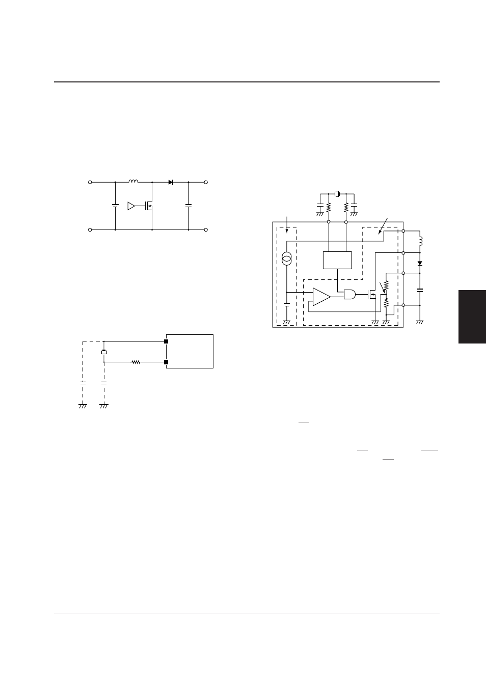
Basic Voltage Booster Operation
Tr1 switches ON and OFF at the frequency of the clock
pulses from the crystal oscillator. When the transistor is
ON, the circuit stores energy in L. When it is OFF, this
energy flows through D to charge C.
The output voltage regulator regulates the boosted out-
put voltage. This voltage is determined by the level at
point A between the two resistors connecting V
O
and
GND. These series use an on-chip resistor to set the
output at a specified voltage.
Internal Circuits
Crystal oscillator
The S1F76330 series incorporate a crystal oscillator cir-
cuit. An external crystal and drain resistor are used to
generate the booster circuit clock. The crystal oscillator
is connected to C
I
and C
O
as shown in the following
figure.
V
I1
GND
V
O
GND
L
D
Tr1
C
In the S1F76330 series, the crystal oscillator output is
sent to CL
O
as the V
O
system signal. The crystal oscil-
lator circuit is activated by V
I
but, because the output
level is shifted and the output is connected to CL
O
, the
oscillator output cannot be obtained without a voltage at
V
O
. Since the crystal oscillator is activated when an
input voltage is applied, oscillation continues even in
standby mode.
Reference voltage generator and output
voltage regulator
The reference voltage generator regulates V
I1
to gener-
ate a voltage for the voltage regulator circuit.
S1F76330
C
I
C
O
R
D
Crystal
C
D
C
G
Note
In step-up voltage operation, the ripple voltage created
by the switching operation is large relative to the output
voltage described above. This ripple voltage is affected
by external components and load conditions. The user
is advised to check this voltage carefully.
Standby mode
Connecting PS to GND places the chip in standby
mode. In this mode, the crystal oscillator is disabled,
switching off the inductor drive transistor and the volt-
age booster circuit. Typically, PS is connected to RST.
If standby mode is not required, leave PS open as it has
a pull-up resistor.
Output voltage response compensation
The S1F76340 series incorporates a response compen-
sation input. A response compensation capacitor is
connected between V
CONT
and V
O
, allowing the ripple
voltage generated by the boosted output voltage to be
suppressed to a minimum.
Reference
voltage
generator
Crystal
oscillator
Crystal
+
–
A
V
I1
C
G
C
D
V
SW
V
O
GND
Output
voltage regulator