Functional descriptions – Epson Power Supply S1F70000 User Manual
Page 30
S1F76620 Series
S1F70000 Series
EPSON
1–13
Technical Manual
S1F76620
Series
FUNCTIONAL DESCRIPTIONS
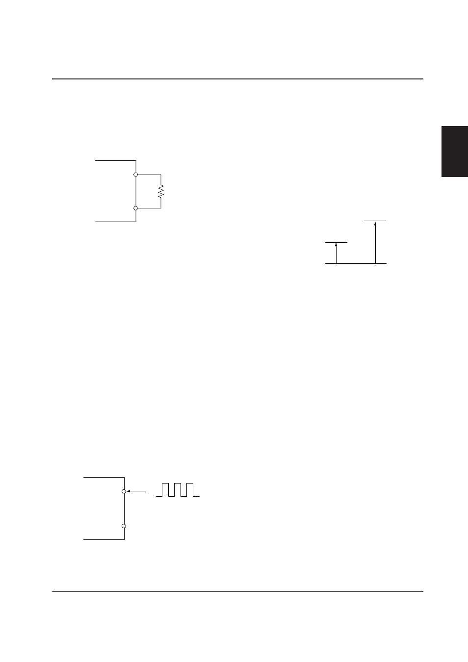
CR Oscillator
S1F76620 has a built-in CR oscillator as the internal os-
cillator, and an external oscillation resistor R
OSC
is con-
nected between the pins OSC1 and OSC2 before opera-
tion.
OSC1
OSC2
R
OSC
(Note 1)
Note 1
Since the oscillation frequency varies with wiring ca-
pacitance, make the cables between the terminals OSC1
and OSC2 and R
OSC
as short as possible.
When setting the external resistor R
OSC
, find R
OSC
suit-
able for f
OSC
that brings about the maximum efficiency
from characteristics graph (9) and (10). The relations
between R
OSC
and f
OSC
in characteristics graph (1) are
expressed approximately with the following formula as
far as the
straight portion (500k
Ω
< R
OSC
< 2M
Ω
) is concerned:
R
OSC
= A • (1/f
OSC
)
(A : Constant, When GND is 0V and V
DD
is 5V, A is
approximately 2.0
×
10
10
(I/F).)
So, the R
OSC
value can be obtained from this formula.
(Recommended oscillation frequency : 10kHz to 30kHz
(R
OSC
: 2M
Ω
to 680k
Ω
))
When the external clock operates, make the pin OSC2
open as shown below and input the 50% duty of the ex-
ternal clock from the pin OSC1.
OSC1
OSC2
External clock
Open
Voltage Conversion Circuit
The voltage conversion circuit uses clocks generated in
the CR oscillator to double the input supply voltage
V
DD
.
In case of 2 times step-up, 2 times voltage (2V
DD
) of
the input voltage is obtained from the V
O
pin when a
pump up capacitor is connected between CAP1+ and
CAP2– and a smoothing capacitor is connected be-
tween V
DD
and V
O
outside.
When GND is 0 and V
DD
is 5, the relations between
input/output and voltage are as shown below:
CAP1=2V
DD
=10V
V
DD
=5V
G
ND
=0V