Epson – Epson Power Supply S1F70000 User Manual
Page 152
S1F76300 Series
S1F70000 Series
EPSON
4–7
Technical Manual
S1F76300
Series
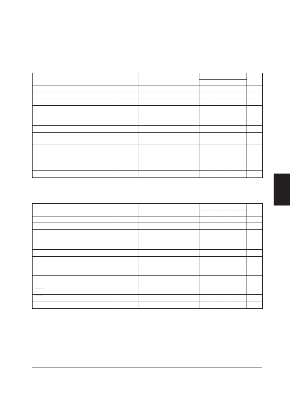
S1F76380M1H0
V
SS
= 0V, Ta = 25 ˚C unless otherwise noted
Parameter
Symbol
Condition
Rating
Unit
Min.
Typ.
Max.
Input voltage
V
I1
0.9
—
2.0
V
Output voltage
V
O
V
l1
= 1.5V
2.10
2.20
2.30
V
Output voltage temperature gradient
Kt
–5.5
–4.5
–3.5
mV/˚C
Detection voltage
V
DET
1.00
1.05
1.10
V
Detection voltage hysteresis ratio
∆
V
DET
—
5
—
%
Operating current
I
DDO
V
I1
= 1.5V, I
O
= 1.0mA
—
7
35
µ
A
Standby current
I
DDS
V
I1
= 1.5V
—
3
10
µ
A
Switching transistor ON resistance
R
SWON
V
I1
= 1.5V, V
O
= 2.2V,
—
7
14
Ω
V
SW
= 0.2V
Switching transistor leakage current
I
SWQ
V
I1
= 1.5V, V
O
= 1.5V,
—
—
0.5
µ
A
V
SW
= 7.0V
RST Low-level output current
I
OL
V
I1
= 0.9V, V
OL
= 0.2V
0.05
0.15
—
mA
PS pullup current
I
IH
V
I1
= 1.5V
—
—
0.5
µ
A
Multiplication clock frequency
f
CLK
V
I1
= 1.5V
25
35
45
kHz
S1F76380M1L0
V
SS
= 0V, Ta = 25 ˚C unless otherwise noted
Parameter
Symbol
Condition
Rating
Unit
Min.
Typ.
Max.
Input voltage
V
I1
0.9
—
2.0
V
Output voltage
V
O
V
l1
= 1.5V
2.30
2.40
2.50
V
Output voltage temperature gradient
Kt
–5.5
–4.0
–3.5
mV/˚C
Detection voltage
V
DET
1.00
1.05
1.10
V
Detection voltage hysteresis ratio
∆
V
DET
—
5
—
%
Operating current
I
DDO
V
I1
= 1.5V, I
O
= 1.0mA
—
7
35
µ
A
Standby current
I
DDS
V
I1
= 1.5V
—
3
10
µ
A
Switching transistor ON resistance
R
SWON
V
I1
= 1.5V, V
O
= 2.4V,
—
7
14
Ω
V
SW
= 0.2V
Switching transistor leakage current
I
SWQ
V
I1
= 1.5V, V
O
= 1.5V,
—
—
0.5
µ
A
V
SW
= 7.0V
RST Low-level output current
I
OL
V
I1
= 0.9V, V
OL
= 0.2V
0.05
0.15
—
mA
PS pullup current
I
IH
V
I1
= 1.5V
—
—
0.5
µ
A
Multiplication clock frequency
f
CLK
V
I1
= 1.5V
25
35
45
kHz