12 i2c interface, 13 jtag interface, 14 interrupts – Artesyn ATCA-9405 Installation and Use (May 2014) User Manual
Page 68: 1 packet processor interrupts, Table 3-5, Cn6880 i2c bus assignment, Packet processor
Packet Processor
ATCA-9405 Installation and Use (6806800M71G)
68
3.12 I2C Interface
The CN6880 has 2 two-wire serial interfaces (TWSI) that provide multi-master and master-
slave I2C mode support. TWSI interface 0 is connected to the four DIMM modules for SPD
detection. TWSI interface 1 is connected to the external EEPROM and to the Glue Logic FPGA
for access to internal status and control registers.
3.13 JTAG Interface
The IEEE 1149.1 compliant JTAG boundary scan interface of CN6880 is connected to an
onboard 16-pin header to support a processor emulator for board debug. The additional
signals for MIPS EJTAG support according to EJTAG Specification Revision 5.0 are supported.
For connector pin out details, refer to
.
3.14 Interrupts
Each Packet Processor is responsible for handling of interrupts that are generated within its
own domain.
3.14.1 Packet Processor Interrupts
The CN6880 includes a central interrupt unit that allows centralized collection of internal and
external interrupts as well as interrupt selection and distribution to the cores and to the
integrated PCI Express controllers.
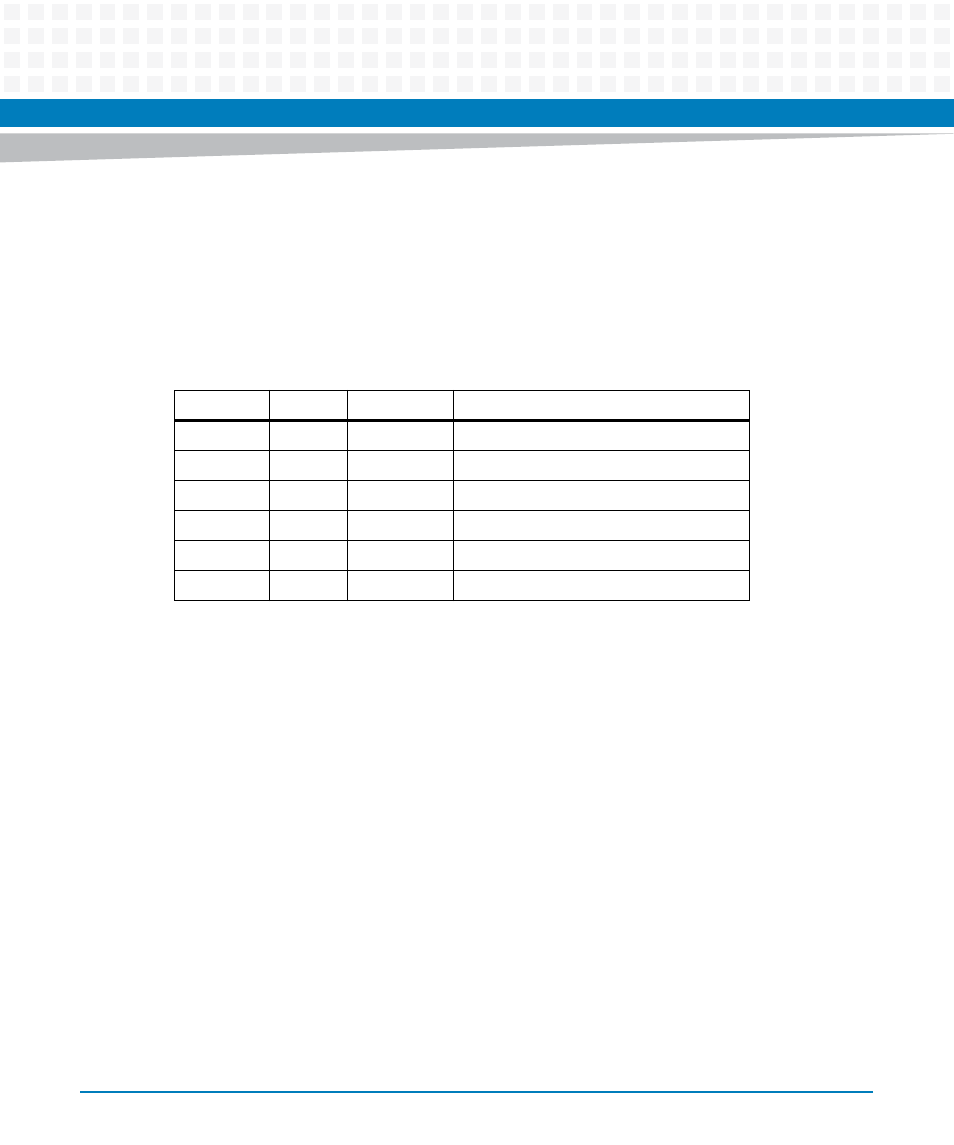
Table 3-5 CN6880 I2C Bus Assignment
Address
TWSI
Component
Function
0xA0
0
NA
DIMM1 Memory Module SPD PROM
0xA2
0
NA
DIMM2 Memory Module SPD PROM
0xA4
0
NA
DIMM3 Memory Module SPD PROM
0xA6
0
NA
DIMM4 Memory Module SPD PROM
0xA0
1
24LC128
U-Boot Parameter Storage EEPROM
0xFE
1
NA
Glue Logic FPGA