Pclk – Altera Stratix V Avalon-ST User Manual
Page 112

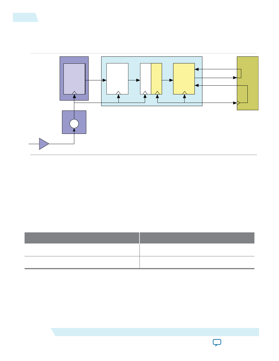
Figure 6-5: Clock Domains and Clock Generation for the Application Layer
The following illustrates the clock domains when using
coreclkout_hip
to drive the Application Layer
and the
pld_clk
of the IP core. The Altera-provided example design connects
coreclkout_hip
to the
pld_clk
. However, this connection is not mandatory.
100 MHz
(or 125 MHz)
refclk
Hard IP for PCI Express
PHY/MAC
Clock
Domain
Crossing
(CDC)
Data Link
and
Transaction
Layers
TX PLL
PCS
250 or 500 MHz
pclk
coreclkout_hip
Application
Layer
pld_clk
(62.5, 125
or 250 MHz)
serdes_pll_locked
pld_core_ready
Transceiver
As this figure indicates, the IP core includes the following clock domains:
pclk
The transceiver derives
pclk
from the 100 MHz
refclk
signal that you must provide to the device.
The PCI Express Base Specification requires that the
refclk
signal frequency be 100 MHz ±300 PPM.
The transitions between Gen1, Gen2, and Gen3 should be glitchless.
pclk
can be turned off for most of
the 1 ms timeout assigned for the PHY to change the clock rate; however,
pclk
should be stable before the
1 ms timeout expires.
Table 6-2: pclk Clock Frequency
Data Rate
Frequency
Gen1
250 MHz
Gen2
500 MHz
The CDC module implements the asynchronous clock domain crossing between the PHY/MAC
pclk
domain and the Data Link Layer
coreclk
domain. The transceiver
pclk
clock is connected directly to the
Hard IP for PCI Express and does not connect to the FPGA fabric.
Related Information
6-6
pclk
UG-01097_sriov
2014.12.15
Altera Corporation
Reset and Clocks
