Seriallite ii megacore pin-out diagrams, Seriallite ii megacore pin-out diagrams –13, Figure 4–12 – Altera SerialLite II IP Core User Manual
Page 67: Arria ii gx/stratix iv phy layer, Transmitter link layer, Receiver layer with no fifo, Receiver link layer with fifo
Chapter 4: Functional Description
4–13
Clocks and Data Rates
January 2014
Altera Corporation
SerialLite II MegaCore Function
User Guide
Arria V, Cyclone V, and Stratix V Transceiver Clocking
For Arria V, Cyclone V, and Stratix V configurations, you must integrate the
transceiver to the SerialLite II MegaCore function manually.
When you configure the transceiver to work in more than 1 lane per SerialLite II
instance, the
tx_clkout(0)
signal from the TX channel (PHY IP) must drive the
SerialLite II input clock (tx_coreclk) and the input port (tx_coreclkin) of all TX
channels (PHY IP). Similarly, if your design requires more than 1 RX channel per
SerialLite II instance, the
rx_clkout(0)
from the RX channel (PHY IP) must drive the
SerialLite II input clock (rx_coreclk) and the input port (rx_coreclkin) of all RX
channels (PHY IP).
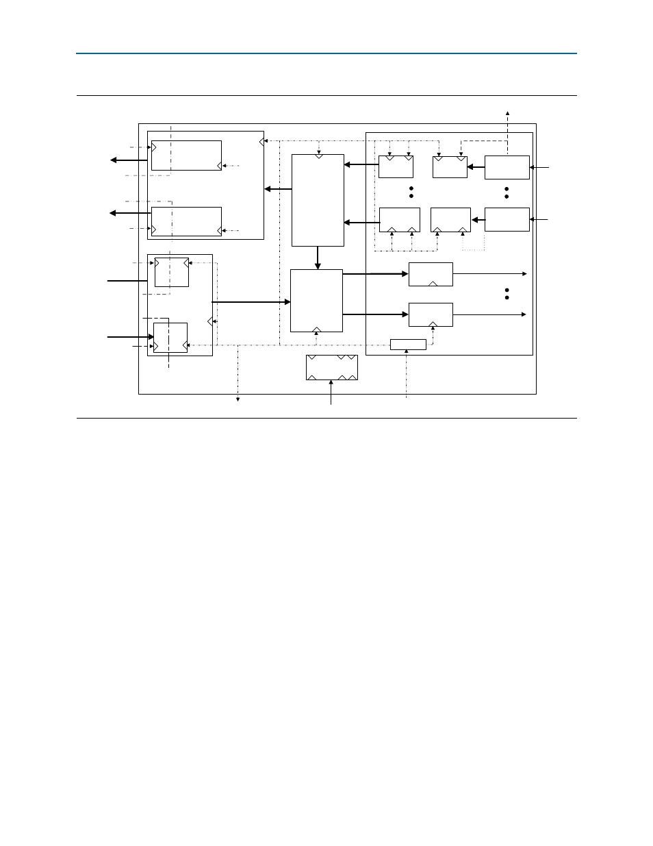
SerialLite II MegaCore Pin-Out Diagrams
This section shows pin-out diagrams for the SerialLite II MegaCore function. The
following diagrams are included:
■
Arria II GX/Stratix IV PHY Layer
■
■
■
Figure 4–12. Full Featured Clock Structure for 5G Symmetrical With TSIZE = 2
XCVR
TX Core
n-bit
n-bit
RX Core
n-bit
Atlantic
#n SLITE2
High
Speed
Links
#m SLITE2
High
Speed
Links
Atlantic
Atlantic
Atlantic
Regular
Priority
Priority
Regular
PComp_
FIFO_0
Byte
serializer
Byte
serializer
PComp_
FIFO_n-1
Byte
deserializer
Byte
deserializer
n-bit
rxrdp_clk
rxhpp_clk
txhpp_clk
txrdp_clk
tx_coreclk
rcvd_clkn-1
mreset_n
Reset Sync
tx_coreclock
rcvd_clk_out[n-1:0]
ATLFIFO
ATLFIFO
ATLFIFO
ATLFIFO
tx_coreclock
Word Aligner (&
Training Pattern
Detection),
[Link State
Machine]
Training
Generator [Link
State Machine]
trefclk
TXPLL
tx_coreclock
tx_coreclock
tx_coreclock
tx_coreclock
RM_
FIFO_0
RM_
FIFO_n-1
slite2_top