Clock compensation, Lane polarity and order reversal, Lane polarity – Altera SerialLite II IP Core User Manual
Page 33: Lane polarity –10, Figure 3–9
3–10
Chapter 3: Parameter Settings
Physical Layer Configuration
SerialLite II MegaCore Function
January 2014
Altera Corporation
User Guide
Clock Compensation
The clock compensation value determines when the clock compensation sequence is
inserted into, or deleted from, the high-speed serial data stream to compensate for
ppm frequency differences between different clock crystals when the Clock
Compensation
option is enabled.
The frequency offset removal (foffre) block includes a FIFO buffer overflow status
output signal: err_rr_foffre_oflw. If this signal toggles, you may need to adjust the
ppm setting.
1
The Clock Compensation option is disabled if the value chosen for the Reference
Clock Frequency
option does not equal data rate/ (transfer size* 10), and the
Receiver Only
port type option is turned on.
Lane Polarity and Order Reversal
The SerialLite II protocol optionally allows the link to recover from some connection
problems. Lane polarity and lane order are reversed automatically.
Lane Polarity
Each lane consists of a differential pair of signals. It is possible for the positive and
negative sides of this pair to be reversed because of a layout error or because it
simplifies layout. The SerialLite II logic can compensate for such a reversed lane on
the receive side. This reversal occurs during link initialization and remains in place for
as long as the link is active.
For training sequence one, the TID field normally read as /T1/ (D10.2) is read as
/!T1/ (D21.5) when the lane polarity is inverted. Likewise for training sequence two,
the TID field normally read as /T2/ (D5.2) is read as /!T2/ (D26.5) when the lane
polarity is inverted. In these training sequences, the /COM/ character is followed by
seven valid data characters. The last character of the sequence is used to determine
the parity. If any of the parity identifiers in any lane is either /!T1/ (D21.5) or /!T2/
(D26.5), the receiver for that lane inverts the polarity.
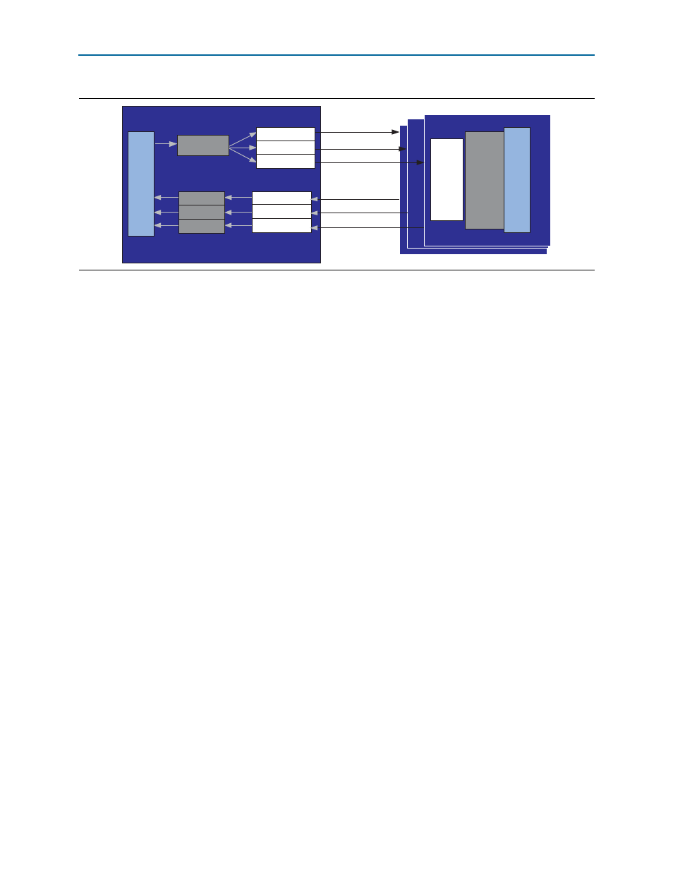
Figure 3–9. Streaming Broadcast Mode Block Diagram
Master FPGA
Broadcast message
Broadcast message
Broadcast message
N-return
lanes
Atlantic
Interface
Shared TX
PHY
RX PHY 1
RX PHY 2
RX PHY N
TX Tsvr 1
TX Tsvr 2
TX Tsvr N
RX Tsvr 1
RX Tsvr 2
RX Tsvr N
Slave FPGA N
PHY
Layer
CDR
SERDES
Atlantic
Interface