Pin descriptions – Cirrus Logic CS42L56 User Manual
Page 8
8
DS851F2
CS42L56
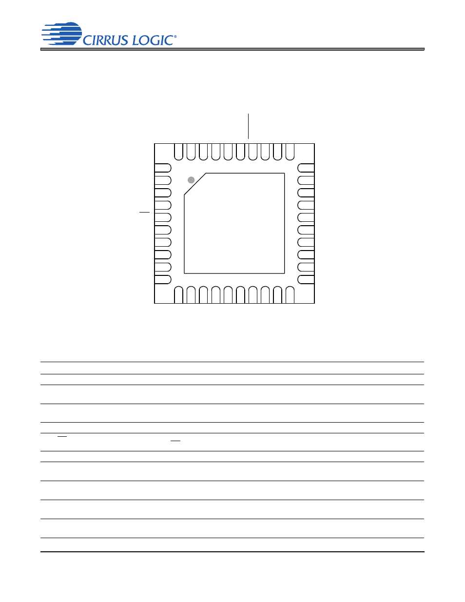
1. PIN DESCRIPTIONS
Pin Name
#
Pin Description
SDIN
1
Serial Audio Data Input (Input) - Input for two’s complement serial audio data.
LRCK
2
Left Right Clock (Input/Output) - Determines which channel, Left or Right, is currently active on the
serial audio data lines.
SDA/CDIN
3
Serial Control Data (Input/Output) - SDA is the bidirectional data pin for the I²C control interface.
CDIN is the input data pin for the SPI control interface.
SCL/CCLK
4
Serial Control Port Clock (Input) - Serial clock for the I²C and SPI control interfaces.
AD0/CS
5
Chip Address (I²C) / Chip Select (SPI) (Input) - For I²C operation, this pin must remain static high
or low. For SPI, CS is the chip-select pin.
VCP
6
Step-Down Charge Pump Power (Input) - Power supply for the step-down charge pump.
FLYP
7
Charge Pump Cap Positive Node (Output) - Positive node for the step-down charge pump’s flying
capacitor.
+VHPFILT
8
Step-Down Charge Pump Filter Connection (Output) - Power supply from the step-down charge
pump that provides the positive rail for the headphone and line amplifiers
FLYC
9
Charge Pump Cap Common Node (Output) - Common positive node for the step-down and invert-
ing charge pumps’ flying capacitors.
FLYN
10
Charge Pump Cap Negative Node (Output) - Negative node for the inverting charge pump’s flying
capacitor.
12
11
13
14
15
16
17
18
19
20
29
30
28
27
26
25
24
23
22
21
39
40
38
37
36
35
34
33
32
31
2
1
3
4
5
6
7
8
9
10
GND/Thermal Pad
VDFILT
VL
SDOUT
MCL
K
SDIN
SC
LK
-VH
P
FI
LT
HPREF
HP
OUTB
TSTN
LINEOUTB
VA
AGND
AFILTB
SDA/CDIN
SCL/CCLK
AD0/CS
+VHPFILT
RESET
FLYC
FLYN
FILT+
AIN2A
MICBIAS
AIN1REF/AIN3A
AFILTA
AIN1A
AIN1B
VQ
FLYP
LRCK
VLDO
VCP
HPOUTA
TSTN
LINEOUTA
LINEREF
AIN2B
HPD
E
TE
CT
AI
N2
REF/
AI
N3
B
Top-Down (Through-Package) View
40-Pin QFN Package