Figure 35. control port timing, i²c write, Figure 36. control port timing, i²c read, 3 memory address pointer (map) – Cirrus Logic CS42L56 User Manual
Page 54: 1 map increment (incr), Figure 35, Figure 36, Cs42l56
54
DS851F2
CS42L56
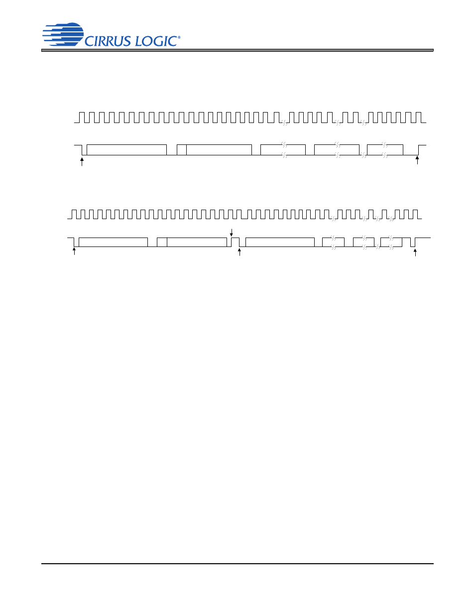
register pointed to by the MAP will be output. Setting the auto-increment bit in MAP allows successive
reads or writes of consecutive registers. Each byte is separated by an acknowledge bit. The ACK bit is
output from the CS42L56 after each input byte is read and is input to the CS42L56 from the microcontrol-
ler after each transmitted byte.
Since the read operation cannot set the MAP, an aborted write operation is used as a preamble. As shown
in
, the write operation is aborted (after the acknowledge for the MAP byte) by sending a stop
condition. The following pseudocode illustrates an aborted write operation followed by a read operation.
Send start condition.
Send 10010100 (chip address & write operation).
Receive acknowledge bit.
Send MAP byte, auto-increment off.
Receive acknowledge bit.
Send stop condition, aborting write.
Send start condition.
Send 10010101 (chip address & read operation).
Receive acknowledge bit.
Receive byte, contents of selected register.
Send acknowledge bit.
Send stop condition.
Setting the auto-increment bit in the MAP allows successive reads or writes of consecutive registers. Each
byte is separated by an acknowledge bit.
4.13.3 Memory Address Pointer (MAP)
The MAP byte comes after the address byte and selects the register to be read or written. Refer to the
pseudo code above for implementation details.
4.13.3.1 Map Increment (INCR)
The device has MAP auto-increment capability enabled by the INCR bit (the MSB) of the MAP. If INCR is
set to 0, MAP will stay constant for successive I²C writes or reads. If INCR is set to 1, MAP will auto-in-
crement after each byte is read or written, allowing block reads or writes of successive registers.
4 5 6 7
24 25
SCL
CHIP ADDRESS (WRITE)
MAP BYTE
DATA
DATA +1
START
ACK
STOP
ACK
ACK
ACK
1 0 0 1 0 1 AD0 0
SDA
INCR
6 5 4 3 2 1 0
7 6 1 0
7 6 1 0
7 6 1 0
0 1 2 3
8 9
12
16 17 18 19
10 11
13 14 15
27 28
26
DATA +n
Figure 35. Control Port Timing, I²C Write
SCL
CHIP ADDRESS (WRITE)
MAP BYTE
DATA
DATA +1
START
ACK
STOP
ACK
ACK
ACK
1 0 0 1 0 1 AD0 0
SDA
1 0 0 1 0 1 AD0 1
CHIP ADDRESS (READ)
START
INCR
6 5 4 3 2 1 0
7 0
7 0
7 0
NO
16
8 9
12 13 14 15
4 5 6 7
0 1
20 21 22 23 24
26 27 28
2 3
10 11
17 18 19
25
ACK
DATA + n
STOP
Figure 36. Control Port Timing, I²C Read