13 control port operation, 1 spi control, Figure 34. control port timing in spi mode – Cirrus Logic CS42L56 User Manual
Page 53: 2 i²c control, 1 spi control 4.13.2 i²c control, Figure 34.control port timing in spi mode, Cs42l56
DS851F2
53
CS42L56
4.13 Control Port Operation
The control port is used to access the registers allowing the CODEC to be configured for the desired oper-
ational modes and formats. The operation of the control port may be completely asynchronous with respect
to the audio sample rates. However, to avoid potential interference problems, the control port pins should
remain static if no operation is required.
The device enters software mode only after a successful write command using one of two software proto-
cols: SPI or I²C, with the device acting as a slave. The SPI protocol is permanently selected whenever there
is a high-to-low transition on the AD0/CS pin after reset. If using the I²C protocol, pin AD0/CS should be
permanently connected to either VL or GND; this option allows the user to slightly alter the chip address as
desired.
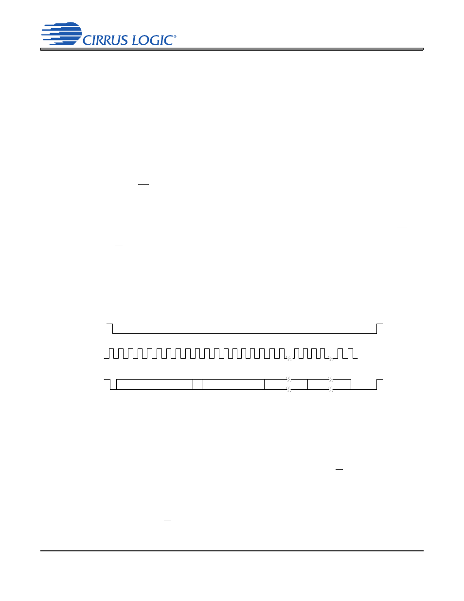
4.13.1 SPI Control
In Software Mode, CS is the CS42L56 chip-select signal, CCLK is the control port bit clock (input into the
CS42L56 from the microcontroller), CDIN is the input data line from the microcontroller. Data is clocked
in on the rising edge of CCLK. The CODEC will only support write operations. Read request will be ig-
nored.
shows the operation of the control port in Software Mode. To write to a register, bring CS low.
The first seven bits on CDIN form the chip address and must be 1001010. The eighth bit is a read/write
indicator (R/W), which should be low to write. The next eight bits form the Memory Address Pointer (MAP),
which is set to the address of the register that is to be updated. The next eight bits are the data which will
be placed into the register designated by the MAP.
There is MAP auto-increment capability, enabled by the INCR bit in the MAP register. If INCR is a zero,
the MAP will stay constant for successive read or writes. If INCR is set to a 1, the MAP will auto-increment
after each byte is read or written, allowing block reads or writes of successive registers.
4.13.2 I²C Control
SDA is a bidirectional data line. Data is clocked into and out of the part by the clock, SCL. The signal tim-
ings for a read and write cycle are shown in
and
. A Start condition is defined as a
falling transition of SDA while the clock is high. A Stop condition is defined as a rising transition of SDA
while the clock is high. All other transitions of SDA occur while the clock is low. The first byte sent to the
CS42L56 after a Start condition consists of a 7-bit chip address field and a R/W bit (high for a read, low
for a write).
The upper 6 bits of the address field are fixed at 100101. Pin ADO forms the least significant bit of the
chip address and should be connected to VL or DGND as desired. To communicate with the CS42L56,
the chip address field, which is the first byte sent to the CS42L56, should match 100101+AD0. The eighth
bit of the address is the R/W bit. If the operation is a write, the next byte is the Memory Address Pointer
(MAP); the MAP selects the register to be read or written. If the operation is a read, the contents of the
4 5 6 7
CCLK
CHIP ADDRESS (WRITE)
MAP BYTE
DATA
1 0 0 1 0 1 0 0
CDIN
INCR
6 5 4 3 2 1 0
7 6 1 0
0 1 2 3
8 9
12
16 17
10 11
13 14 15
DATA +n
CS
7 6 1 0
Figure 34. Control Port Timing in SPI Mode