1 pseudo-differential inputs, Figure 14. stereo pseudo-differential input, 2 large-scale inputs – Cirrus Logic CS42L56 User Manual
Page 32: Table 1. input voltage pga settings, Figure 14.stereo pseudo-differential input, Cs42l56
32
DS851F2
CS42L56
4.2.1
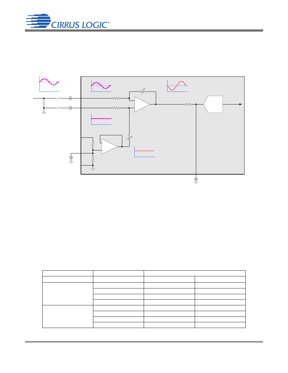
Pseudo-differential Inputs
The CS42L56 implements a pseudo-differential input stage. The AINxREF inputs are intended to be used
as a pseudo-differential reference signal. This feature provides common mode noise rejection with single-
ended signals.
shows a basic diagram outlining the internal implementation of the pseudo-dif-
ferential input stage, including a recommended stereo pseudo-differential input topology. If pseudo-differ-
ential input functionality is not required, the AINxREF pin should be AC-coupled to GND.
It should be noted that the AINxREF inputs are intended to be used solely to provide a low-level, pseudo-
differential reference signal for the internal input amplifiers when in pseudo-differential mode. Using the
analog input pins in a fully differential configuration by providing a large signal on the AINxREF pin is not
recommended. The output of the PGA will clip if the voltage difference between AINxx and AINxREF ex-
ceeds the full-scale voltage specification (See
).
4.2.2
Large-scale Inputs
The CS42L56 allows the user to input signals that would be larger than the ADC full-scale input voltage
by using the PGA to attenuate the signal prior to going to the ADC.
shows the PGA gain setting
needed to stay under the maximum ADC input voltage.
Supply Voltage
PGA Gain Setting
Maximum Input Voltage
(V)
(dB)
(mV
RMS
)
(V
PP
)
1.8
0.0
509
1.44
-0.5
539
1.52
-1.0
571
1.62
-1.5
604
1.71
2.5
0.0
707
2.00
-0.5
748
2.12
-1.0
793
2.24
-1.5
840
2.38
Table 1. Input Voltage PGA Settings
xIN
xREF
Signal+
Anti-
Aliasing
Filter
Common-Mode Cancellation,
Invert, and Gain
AFILTx
DC-Block
VA
VQ
AGND
VCM
R
R
ADC
Parallel PCB
traces from
signal source
Digital
Full Scale
VCM
VCM
V=?
VCM
VCM
-
+
-
+
Figure 14. Stereo Pseudo-Differential Input