See figure 47). t, Ee figure 47), Figure 47 – Intel 815 User Manual
Page 96: Agp/display cache design guidelines, 96 intel
AGP/Display Cache Design Guidelines
R
96
Intel
®
815 Chipset Platform Design Guide
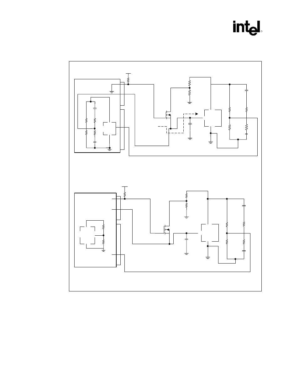
Figure 47. AGP 2.0 VREF Generation and Distribution
C8
500 pF
AGP
Device
1.5V AGP
Card
VDDQ
GND
R9
300
Ω
1%
R2
200
Ω
1%
C9
0.1 uF
VDDQ
REF
GND
GMCH
C8
500 pF
REF
U6
mosfet
R7
1 K
Ω
+12V
TYPEDET#
VrefCG
VrefGC
VDDQ
Notes:
1. The resistor dividers should be placed near the GMCH. The AGPREF signal must be 5 mils wide and routed 10 mils from adjacent signals.
2. R7 is the same resistor seen in AGP VDDQ generation example circuit figure (R1)
AGP
Device
3.3V AGP
Card
VDDQ
GND
C10
0.1 uF
VDDQ
REF
GND
GMCH
R6
1 K
Ω
R2
1 K
Ω
R5
82
Ω
R4
82
Ω
REF
U6
mosfet
+12V
TYPEDET#
VrefCG
VrefGC
VDDQ
The resistor dividers should be placed near the GMCH. The AGPREF signal must be 5 mils wide and routed 25 mils from adjacent signals.
C9
500 pF
R9
300
Ω
1%
R2
200
Ω
1%
agp_2.0ref_gen_dist
b) 3.3V AGP Card
a) 1.5V AGP Card
R6
1 K
Ω
R5
82
Ω
R2
1 K
Ω
R4
82
Ω
C9
500 pF
(See note 2)
R7
1 K
Ω
(See note 2)
The flexible VREF divider shown in Figure 47 uses a FET switch to switch between the locally
generated VREF (for 3.3V add-in cards) and the source-generated VREF (for 1.5V add-in cards).
Use of the source-generated VREF at the receiver is optional and is a product implementation
issue beyond the scope of this document.