Secondary ide connector requirements, 4 secondary ide connector requirements – Intel 815 User Manual
Page 117
I/O Subsystem
R
Intel
®
815 Chipset Platform Design Guide
117
10.2.4
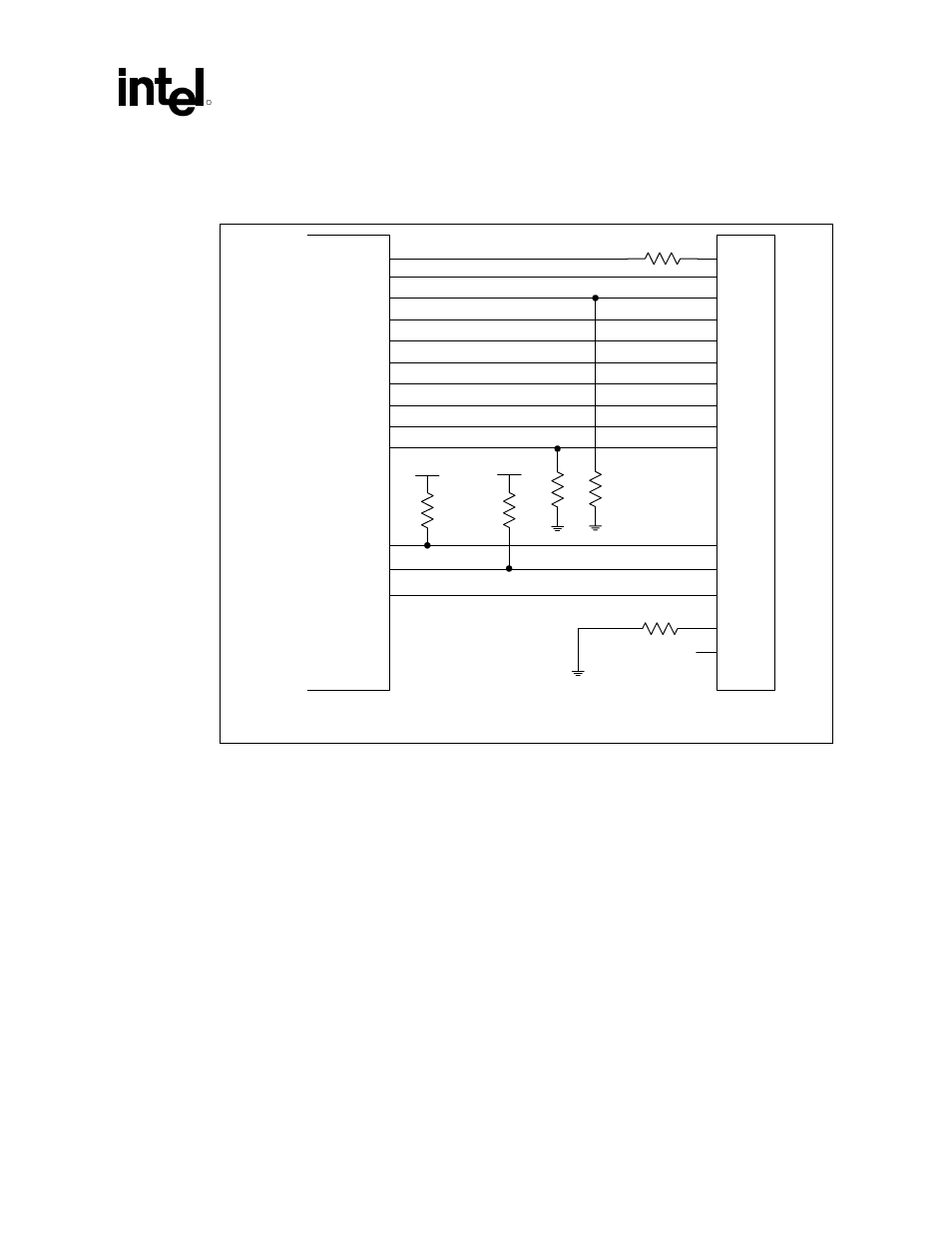
Secondary IDE Connector Requirements
Figure 61. Resistor Schematic for Secondary IDE Connectors
5.6
k
Ω
Reset#
S
econ
da
ry I
D
E
co
nn
ect
or
ICH
10 k
Ω
SDD[15:8]
SDD[6:0]
PCIRST_BUF#*
22 - 47
Ω
SDA[2:0]
SDCS1#
SDCS3#
SDIOR#
SDIOW#
SDDREQ
SIORDY
SDD[7]
* Due to high loading, PCIRST# must be buffered.
1 k
Ω
5V
470
Ω
CSEL
Pin 32
N.C.
SDDACK#
IRQ15
5V
8.2 k
Ω
IDE_resistor_schem_secondary
•
Due to the elimination of the ISA bus from the ICH, PCI_RST# should be connected to pin 1
of the IDE connectors as the IDE reset signal. Because of high loading, the PCI_RST# signal
should be buffered.
•
22
Ω
to 47
Ω
series resistors are required on RESET#. The correct value should be
determined for each unique motherboard design, based on signal quality.
•
IRQ14 and IRQ15 each require an 8.2 k
Ω
pull-up resistor to VCC.
•
A 1 k
Ω
pull-up to 5V is required on PIORDY and SIORDY.
•
A 470
Ω
pull-down is required on pin 28 of each connector.
•
A 5.6 k
Ω
pull-down is required on PDREQ and SDREQ.
•
The primary IDE connector uses IRQ14, and the secondary IDE connector uses IRQ15.
•
There is no internal pull-up or pull-down on PDD7 or SDD7 of the ICH. Devices must not
have a pull-up resistor on DD7. It is recommended that a host have a 10 k
Ω
pull-down resistor
on PDD7 and SDD7 to allow the host to recognize the absence of a device at power-up (as
required by the ATA-4 specification).