Processor design requirements, Designs using a-2 gmch, 2 processor design requirements – Intel 815 User Manual
Page 31
Universal Socket 370 Design
R
Intel
®
815 Chipset Platform Design Guide
31
Table 4. Clock Synthesizer Considerations for Universal Socket 370 Design
Signal
Issue
Implementation For
Universal Socket 370 Design
VDD Intel
®
CK-815 does not support
VTTPWRGD
Addition of FET switch which supplies power
to VDD only when VTTPWRGD is asserted.
Note:
FET must have no more than
100 milliohms resistance between
source and drain.
4.2 Processor
Design
Requirements
4.2.1
Use of Universal Socket 370 Design with Incompatible
GMCH
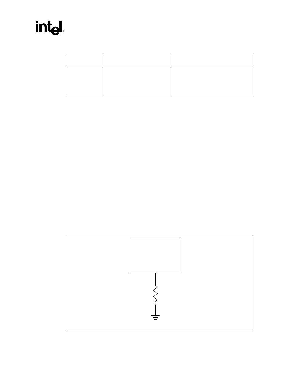
The universal socket 370 design is intended for use with the Intel 815 chipset platform for use with
the universal socket 370. A universal socket 370 design populated with an earlier stepping of the
GMCH is not compatible with future 0.13 micron socket 370 processors and, if used, will cause
eventual failure of these processors. To prevent a future 0.13 micron socket 370 processor from
being used with an incompatible stepping of the GMCH, the recommendation is to lay out the site
for a 0
Ω
pull-down to ground on processor pin AJ3. This pin is a RESET# signal on future
0.13 micron socket 370 processors and, by populating the resistor, these future processors will be
prevented from functioning when placed in a board with an incompatible stepping of the GMCH.
All Pentium III (CPUID=068xh) and Celeron (CPUID=068xh) processors will continue to boot
normally. Not populating the resistor will allow future 0.13 micron socket 370 processors to boot.
Refer to Figure 7 for an example implementation.
Figure 7. Future 0.13 Micron Socket 370 Processor Safeguard for Universal Socket 370
Designs Using A-2 GMCH
Future 0.13 Micron
Socket 370
Processors
AJ3
0
Ω
Tual_pin_aj3