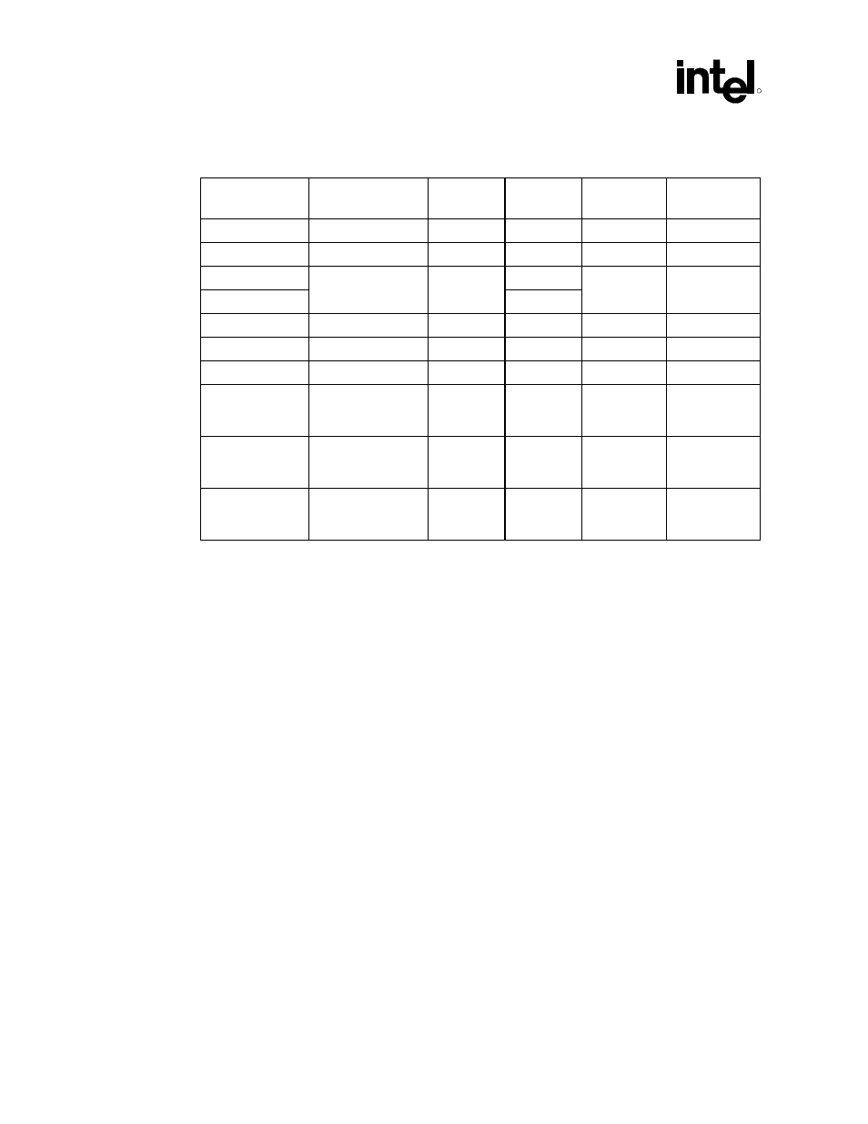
Table 30. simulated clock routing solution space, General clock layout guidelines – Intel 815 User Manual
Page 136
Clocking
R
136
Intel
®
815 Chipset Platform Design Guide
Table 30. Simulated Clock Routing Solution Space
Destination Topology
from
Previous Figure
Section 0
Length
Section 1
Length
Section 2
Length
Section 3
Length
SDRAM MCLK
Layout 5
N/A
< 0.5”
A
1
N/A
GMCH SCLK
3
Layout 2
N/A
< 0.5”=L1
A + 3.5” – L1
0.5”
Processor BCLK
< 0.5”
GMCH HCLK
Layout 3
< 0.1”
<0.5”
A + 5.2”
A + 8”
GMCH HUBCLK
Layout 4
N/A
<0.5”
A + 8”
N/A
ICH HUBCLK
Layout 4
N/A
<0.5”
A + 8”
N/A
ICH PCICLK
Layout 4
N/A
<0.5”
A + 8”
N/A
AGP CLK
Layout 4
N/A
<0.5”
A + 3”
to
A + 4”
N/A
PCI down
2
Layout 4
N/A
<0.5”
A + 8.5”
to
A + 14”
N/A
PCI slot
2
Layout 1
N/A
<0.5”
A + 5”
to
A + 11”
NOTES:
1. Length “A” has been simulated up to 6 inches. The length must be matched between SDRAM MCLK
lines by ±100 mils.
2. All PCI clocks must be within 6 inches of the ICH PCICLK route length. Routing on PCI add-in cards
must be included in this length. In the presented solution space, the ICH PCICLK was considered to be
the shortest in the 6 inches trace routing range, and other clocks were adjusted from there. The system
designer may choose to alter the relationship of PCI device and slot clocks, as long as all PCI clock
lengths are within 6 inches. Note that the ICH PCICLK length is fixed to meet the skew requirements of
the ICH PCICLK to ICH HUBCLK.
3. 22 pF Load capacitor should be placed 0.5 inch from GMCH Pin.
General Clock Layout Guidelines
•
All clocks should be routed 5 mils wide with 15-mil spacing to any other signals.
•
It is recommended to place capacitor sites within 0.5 inch of the receiver of all clocks. They
are useful in system debug and AC tuning.
•
Series resistor for clock guidelines: 22
Ω
for GMCH SCLK and SDRAM clocks. All other
clocks use 33
Ω
.
•
Each DIMM clock should be matched within ±10 mils.