Agp 2.0, 2 agp 2.0 – Intel 815 User Manual
Page 82
AGP/Display Cache Design Guidelines
R
82
Intel
®
815 Chipset Platform Design Guide
ECR #48 can be viewed on the Intel Web site at:
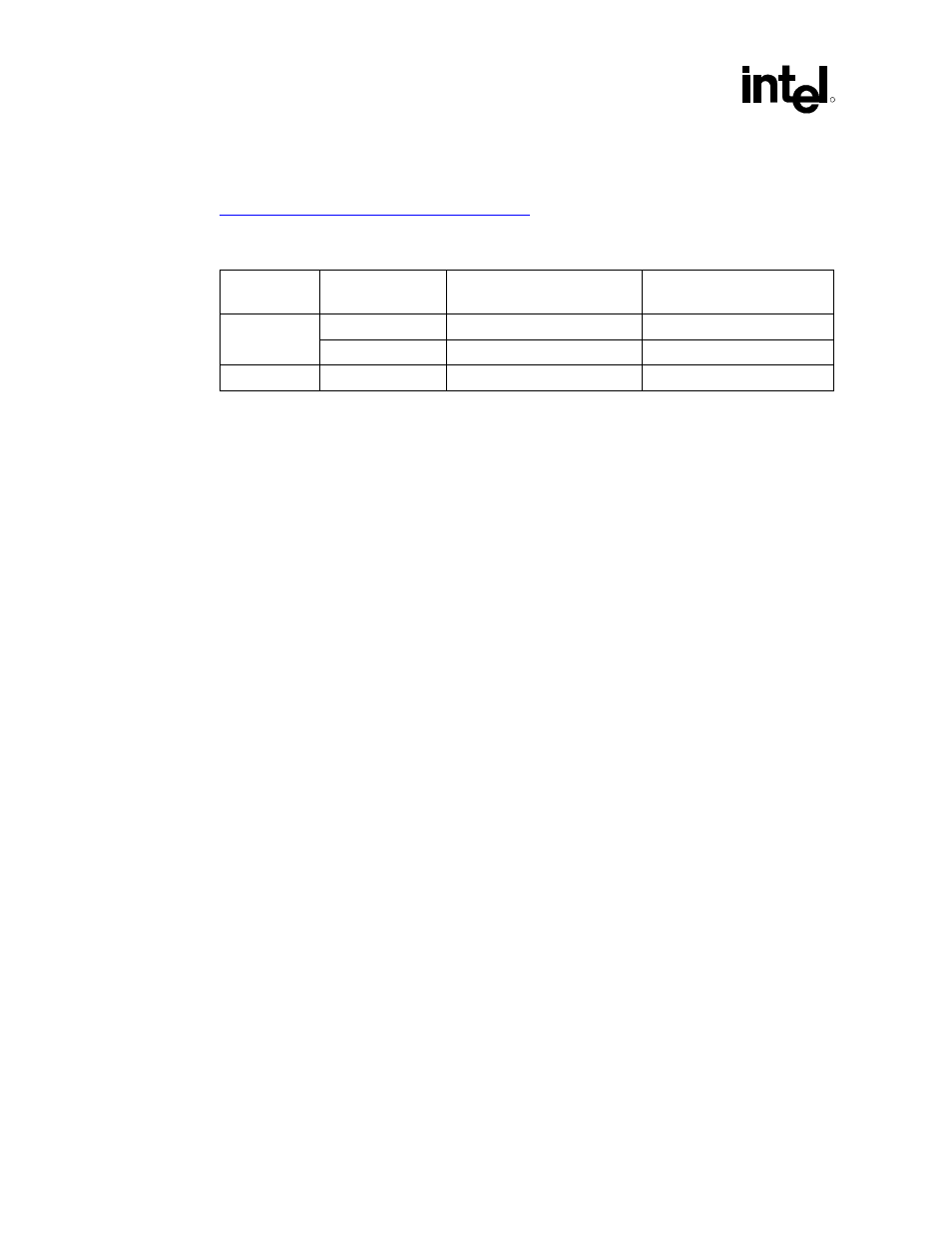
More information regarding this component (AGP RM) is available from the following vendors.
Resin Color
Supplier Part
Number
“Left Handed” Orientation
(Preferred)
“Right Handed” Orientation
(Alternate)
AMP P/N
136427-1
136427-2
Black
Foxconn P/N
006-0002-939
006-0001-939
Green Foxconn
P/N 009-0004-008
009-0003-008
7.2 AGP
2.0
The AGP Interface Specification, Revision 2.0 enhances the functionality of the original AGP
Interface Specification, Revision 1.0 by allowing 4X data transfers (4 data samples per clock) and
1.5V operation. The 4X operation of the AGP interface provides for “quad-pumping” of the AGP
AD (address/data) and SBA (side-band addressing) buses. That is, data is sampled four times
during each 66 MHz AGP clock, which means that each data cycle is ¼ of a 15 ns (66 MHz)
clock, or 3.75 ns. Note that 3.75 ns is the data cycle time, not the clock cycle time. During 2X
operation, data is sampled twice during a 66 MHz clock cycle, so the data cycle time is 7.5 ns. To
allow for such high-speed data transfers, the 2X mode of AGP operation uses source-synchronous
data strobing. During 4X operation, the AGP interface uses differential source-synchronous
strobing.
With data cycle times as small as 3.75 ns and setup/hold times of 1 ns, propagation delay
mismatch is critical. In addition to reducing propagation delay mismatch, it is important to
minimize noise. Noise on the data lines causes the settling time to be long. If the mismatch
between a data line and the associated strobe is too great or if there is noise on the interface,
incorrect data will be sampled. The low-voltage operation on the AGP (1.5V) requires even more
noise immunity. For example, during 1.5V operation, V
ilmax
is 570 mV. Without proper isolation,
cross-talk could create signal integrity issues.