Figure 40. intel, 815 chipset platform decoupling example – Intel 815 User Manual
Page 76
System Memory Design Guidelines
R
76
Intel
®
815 Chipset Platform Design Guide
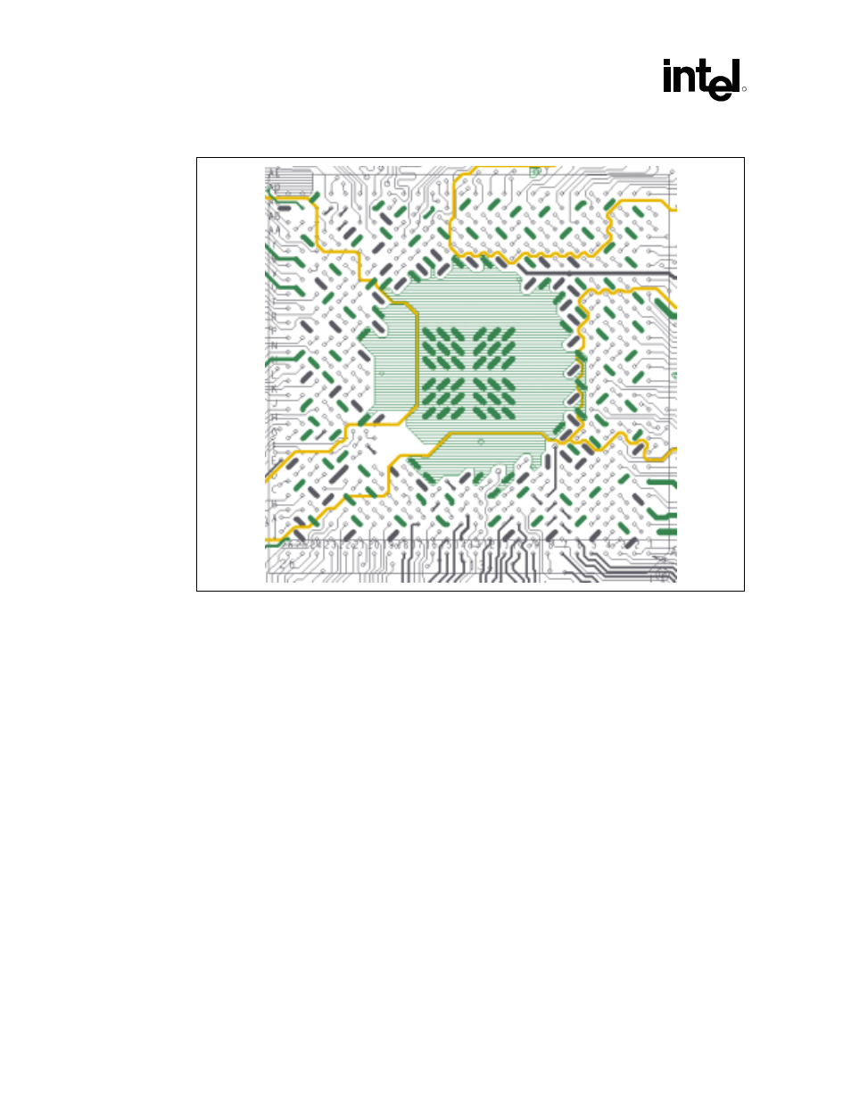
Figure 40. Intel
®
815 Chipset Platform Decoupling Example
Yellow lines in Figure 40 show layer-two plane splits. (Printed versions of this document will
show the layer two plane splits in the left-side, bottom, right-side, and upper-right-side quadrants
enclosed in gray lines.) Note that the layer 1 shapes do NOT cross the plane splits. The bottom
shape is a VSS fill over VddSDRAM. The left-side shape is a VSS fill over VddAGP. The larger
upper-right-side shape is a VSS fill over VddCORE.
Additional decoupling capacitors shown in Figure 41 should be added between the DIMM
connectors to provide a current return path for the reference plane discontinuity created by the
DIMM connectors themselves. One 0.01
µ
F X7R capacitor should be added per every ten
SDRAM signals. Capacitors should be placed between the DIMM connectors and evenly spread
out across the SDRAM interface.
For debug purposes, four or more 0603 capacitor sites should be placed on the backside of the
board, evenly distributed under the Intel 815 chipset platform’s system memory interface signal
field.