Pga370 socket definition details, Table 12. processor pin definition comparison, 4 pga370 socket definition details – Intel 815 User Manual
Page 52
System Bus Design Guidelines
R
52
Intel
®
815 Chipset Platform Design Guide
5.4
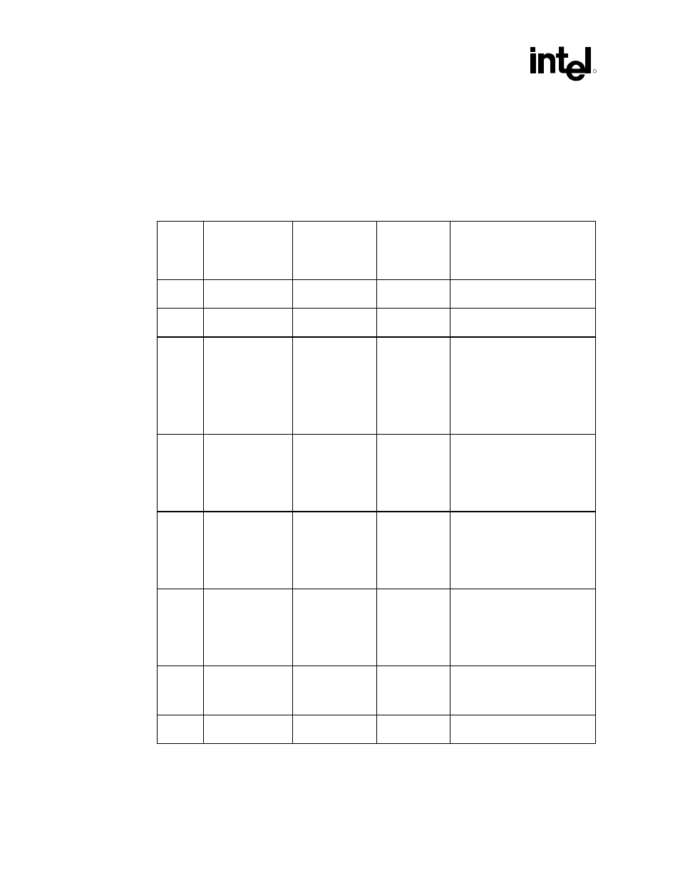
PGA370 Socket Definition Details
The following table compares the pin names and functions of the Intel
processors supported in the
Intel 815 chipset platform for use with the universal socket 370.
Table 12. Processor Pin Definition Comparison
Pin #
Pin Name
Intel
®
Celeron™
Processor
(CPUID=068xh)
Pin Name
Intel
®
Pentium
®
III Processor
(CPUID=068xh)
Pin Name
Future 0.13
Micron
Socket 370
Processors
Function
AA33 Reserved
VTT
VTT
•
AGTL/AGTL+ termination
voltage
AA35 Reserved
VTT
VTT
•
AGTL/AGTL+ termination
voltage
AB36 VCC
CMOS
VCC
CMOS
VTT
•
CMOS voltage level for Intel
®
Pentium
®
III processor
(CPUID=068xh) and Intel
®
Celeron™ processor
(CPUID=068xh).
•
AGTL termination voltage for
future 0.13 micron socket 370
processors.
AD36 VCC1.5
VCC1.5
VTT
•
VCC1.5 for Pentium III
processor (CPUID=068xh)
and Celeron processor
(CPUID=068xh).
•
VTT
for future 0.13 micron
socket 370 processors.
AF36 VSS
VSS
NC
•
Ground for Pentium III
processor (CPUID=068xh)
and Celeron processor
(CPUID=068xh).
•
No connect for future 0.13
micron socket 370 processors.
AG11 VSS
VSS
VTT
•
Ground for Pentium III
processor (CPUID=068xh)
and Celeron processor
(CPUID=068xh).
•
VTT for future 0.13 micron
socket 370 processors
AH4 Reserved
RESET# RESET#
•
Processor reset for the
Pentium III processor (068xh)
and Future 0.13 micron socket
370 processors
AH20 Reserved
VTT
VTT
•
AGTL/AGTL+ termination
voltage