Integrated graphics display output, 104 intel – Intel 815 User Manual
Page 104
Integrated Graphics Display Output
R
104
Intel
®
815 Chipset Platform Design Guide
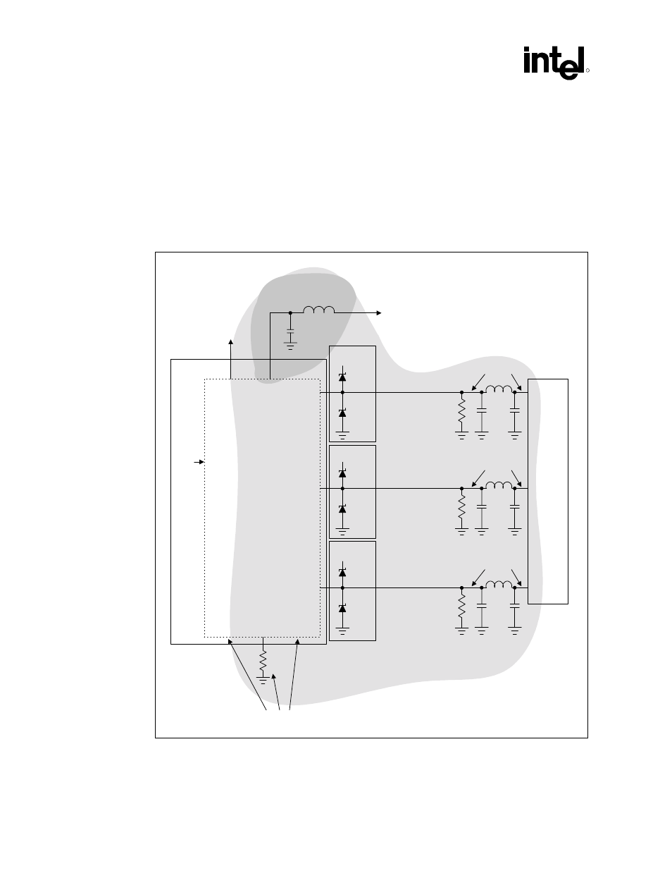
Figure 51 shows the recommended RAMDAC component placement and routing. The termination
resistance can be placed anywhere along the video route from the RAMDAC output to the VGA
connector, as long as the trace impedances are designed as indicated in the following figure. It is
advisable to place the pi-filters in close proximity with the VGA connector, to maximize the EMI
filtering effectiveness. The LC filter components for the RAMDAC/PLL power plane, the
decoupling capacitors, the latch-up protection diodes, and the reference resistor should be placed
in close proximity with the respective pins. Figure 52 shows the recommended reference resistor
placement and the ground connections.
Figure 51. Recommended RAMDAC Component Placement & Routing
RAMDAC
VCCDACA1/
VCCDACA2
VCCDA
Red
Graphics
Chip
Pixel
clock
(from
DPLL)
Cf
Lf
LC
filter
1.8 V board
power plane
Place LC filter components and
high-frequency decoupling
capacitors as close as possible
to power pins
1.8 V board
power plane
Green
Blue
VSSDACA
Analog
power plane
1.8 V
IREF
IWASTE
Place reference
resistor near IREF pin
Rset
VGA
RAMDAC comp placement routing
1.8 V board
power plane
Rt
D2
D1
C1
C2
FB
Pi filter
Red route
37.5
Ω
route
75
Ω
routes
1.8 V board
power plane
Rt
D2
D1
C1
C2
FB
Pi filter
Green route
37.5
Ω
route
75
Ω
routes
1.8 V board
power plane
Rt
D2
D1
C1
C2
FB
Pi filter
Blue route
37.5
Ω
route
75
Ω
routes
Place diodes close to
RGB pins
Avoid routing
toggling signals in
this shaded area
Via straight down to the ground plane
- Match the RGB routes
- Space between the RGB routes a min. of 20 mils
Place pi filter near VGA connector
NOTE:
Diodes D
1
, D
2
are clamping diodes with low leakage and low capacitive loading. An example is:
California Micro Devices PAC DN006 (6 channel ESD protection array).