Processor reset requirements, Figure 25. reset#/reset2# routing guidelines, 8 processor reset requirements – Intel 815 User Manual
Page 58
System Bus Design Guidelines
R
58
Intel
®
815 Chipset Platform Design Guide
5.8
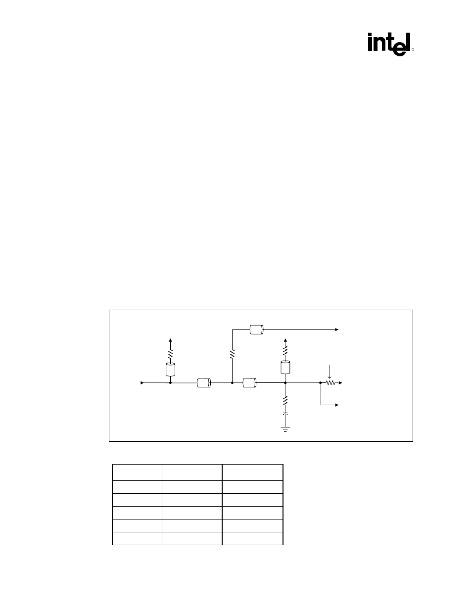
Processor Reset Requirements
Universal PGA370 designs must route the AGTL/AGTL+ reset signal from the chipset to two pins
on the processor as well as to the debug port connector. This reset signal is connected to the
following pins at the PGA370 socket:
•
AH4 (RESET#). The reset signal is connected to this pin for the Pentium III processor
(CPUID=068xh), Celeron processor (CPUID=068xh), and future 0.13 micron socket 370
processors
•
X4 (Reset2# or GND, depending on processor). The X4 pin is RESET2# for Pentium III
processor (CPUID=068xh) and Celeron processor (CPUID=068xh). X4 is GND for future
0.13 micron socket 370 processors. An additional 1k
Ω
resistor is connected in series with pin
X4 to the reset circuitry since pin X4 is a ground pin in future 0.13 micron socket 370
processors.
Note: The AGTL/AGTL+ reset signal must always terminate to VTT on the motherboard.
Designs that do not support the debug port will not utilize the 240
Ω
series resistor or the
connection of RESET# to the debug port connector. RESET2# is not required for platforms that
do not support the Celeron processor (CPUID=068xh). Pin X4 should then be connected to
ground.
The routing rules for the AGTL/AGTL+ reset signal are shown in Figure 25.
Figure 25. RESET#/RESET2# Routing Guidelines
ITP
Pin X4
Processor
Pin AH4
lenITP
VTT
Daisy chain
10 pF
86
Ω
lenCPU
lenCS
91
Ω
cs_rtt_stub
Chipset
VTT
240
Ω
22
Ω
cpu_rtt_stub
sys_bus_reset_routin
1 k
Ω
Table 14. RESET#/RESET2# Routing Guidelines (see Figure 25)
Parameter
Minimum (in)
Maximum (in)
LenCS 0.5 1.5
LenITP 1 3
LenCPU 0.5 1.5
cs_rtt_stub 0.5
1.5
cpu_rtt_stub 0.5
1.5