Usb checklist, Ac ‘97 checklist, 2 usb checklist – Intel 815 User Manual
Page 162: 3 ac ‘97 checklist
System Design Checklist
R
162
Intel
®
815 Chipset Platform Design Guide
13.4.2
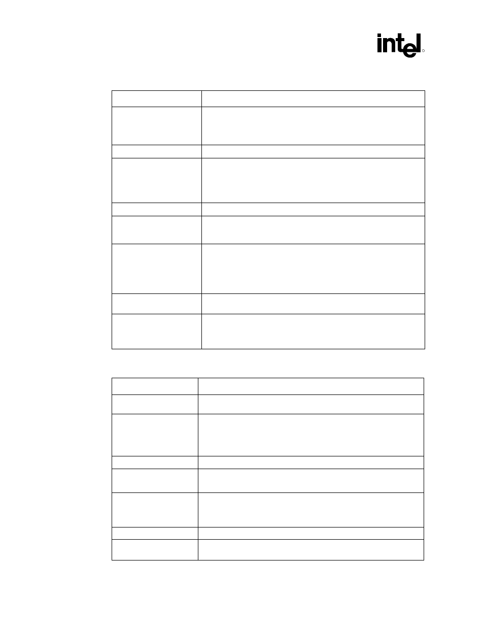
USB Checklist
Checklist Items
Recommendations
USBP0P, USBP0N,
USB_D1_N, USB_D1_P
•
Decouple through a 47 pF capacitor to GND
•
Signal goes through 15 Ω resistor
•
Pull-down through a 15 kΩ resistor to GND
OC#0
•
Connected to AGP/AC97 Circuitry (See Intel CRB Schematic pg. 20)
USB_D2_N, USB_D2_P,
USB_D3_N, USB_D3_P,
USB_D4_N, USB_D4_P,
USBP1P, USBP1N,
USBP0P, USBP0N
•
Pull-down through a 15 kΩ resistor to GND
D-/D+ data lines
•
Use 15
Ω
series resistors.
VCC USB
•
Power off 5V standby if wake on USB is to be implemented IF there is
adequate standby power. It should be powered off of 5 V core instead of
5 V standby if adequate standby power is not available.
Voltage Drop
Considerations
•
The resistive component of the fuses, ferrite beads and traces must be
considered when choosing components and Power/GND trace width.
This must be done such that the resistance between the VCC5 power
supply and the host USB port is minimized. Minimizing this resistance
will minimize voltage drop seen along that path during operating
conditions.
Fuse
•
A minimum of 1A fuse should be used. A larger fuse may be necessary
to minimize the voltage drop.
Voltage Droop
Considerations
•
Sufficient bypass capacitance should be located near the host USB
receptacles to minimize the voltage droop that occurs on the hot attach
of new device. See most recent version of the USB specification for
more information.
13.4.3
AC ‘97 Checklist
Checklist Items
Recommendations
AC_SDOUT
•
Pulled up to VCC3_3 through a 10 K
Ω
resistor and a jumper to AC97
Connector and AC97 codec from ICH.
AC_SDIN0
AC_SDIN1
•
Pull-down through a 10 kΩ resistor to GND. The SDATAIN[0:1] pins
should not be left in a floating state if the pins are not connected and the
AC-link is active – they should be pulled to ground through a weak
(approximately 10 k
Ω
) pull-down resistor (see Section 5.9.3 for more
information).
AC97_OC#
•
Connects to OC# circuitry. (see CRB schematics page 20).
AC_XTAL_OUT,
AC_XTAL_IN
•
Signal comes from Oscillator Y4
•
Decouple through a 22 pF capacitor to GND
PRI_DWN#
•
Connected through jumper to PRI_DWN_U or GND. (see CRB schematic
page 27) If the motherboard implements an active primary codec on the
motherboard and provides and AMR connector, it must tie PRI_DN# to
GND.
PRI_DWN_U
•
Pull-up through a 4.7 kΩ resistor to VCC3SBY
LINE_IN_R
•
From FB9 decouple through a 100 pF NPO capacitor to AGND. Run
signal through 1
µ
F TANT capacitor