Custom solutions, Voltage regulation guidelines, Decoupling guidelines for universal pga370 designs – Intel 815 User Manual
Page 63: Vcccore decoupling design, Core, Decoupling design, Figure 29. core reference model, 10 voltage regulation guidelines, 4 custom solutions, 1 vcc
System Bus Design Guidelines
R
Intel
®
815 Chipset Platform Design Guide
63
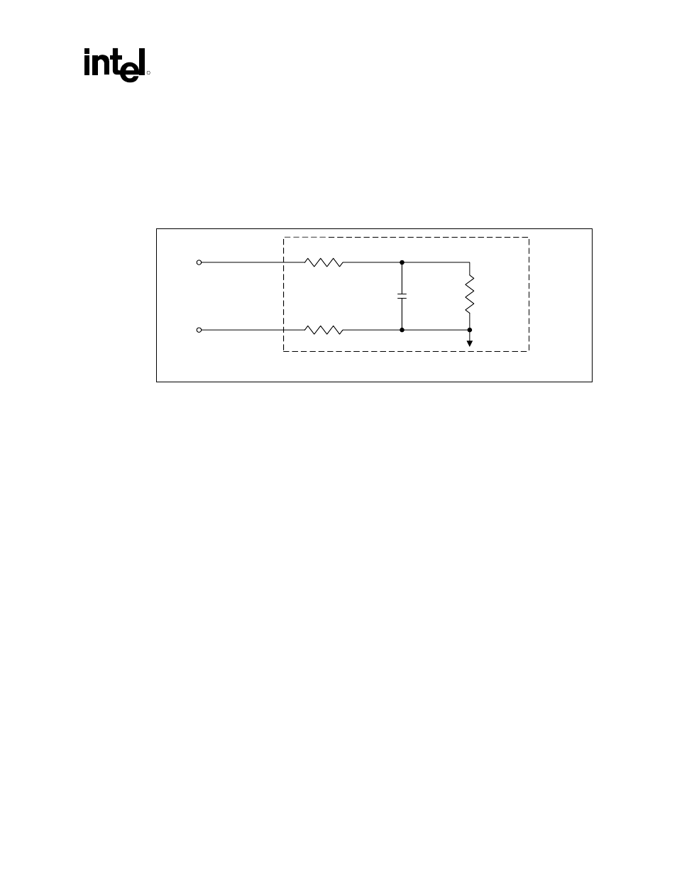
5.9.4 Custom
Solutions
As long as designers satisfy filter performance and requirements as specified and outlined in
Section 5.9.2, other solutions are acceptable. Custom solutions should be simulated against a
standard reference core model (see Figure 29).
Figure 29. Core Reference Model
PLL1
PLL2
sys_bus_core_ref_model
0.1
Ω
0.1
Ω
120 pF
1 k
Ω
Processor
NOTES:
1. 0.1
Ω
resistors represent package routing.
2. 120 pF capacitor represents internal decoupling capacitor.
3. 1 k
Ω
resistor represents small signal PLL resistance.
4. Be sure to include all component and routing parasitics.
5. Sweep across component/parasitic tolerances.
6. To observe IR drop, use DC current of 30 mA and minimum VCC
CORE
level.
7. For other modules (interposer, DMM, etc.), adjust routing resistor if desired, but use minimum numbers.
5.10
Voltage Regulation Guidelines
A universal PGA370 design will need the voltage regulation module (VRM) or on-board voltage
regulator (VR) to be compliant with Intel VRM 8.5 DC-DC Converter Design Guidelines.
5.11
Decoupling Guidelines for Universal PGA370
Designs
These preliminary decoupling guidelines for universal PGA370 designs are estimated to meet the
specifications of VRM 8.5 DC-DC Converter Design Guidelines.
5.11.1 VCC
CORE
Decoupling Design
•
Sixteen or more 4.7
µ
F capacitors in 1206 packages.
All capacitors should be placed within the PGA370 socket cavity and mounted on the primary side
of the motherboard. The capacitors are arranged to minimize the overall inductance between the
VCC
CORE
/VSS power pins, as shown in Figure 30.