Configuring non-vtt processor pins, Figure 12. vttpwrgd configuration circuit, 6 configuring non-vtt processor pins – Intel 815 User Manual
Page 36: Universal socket 370 design, 36 intel, 815 chipset platform design guide
Universal Socket 370 Design
R
36
Intel
®
815 Chipset Platform Design Guide
4.2.6
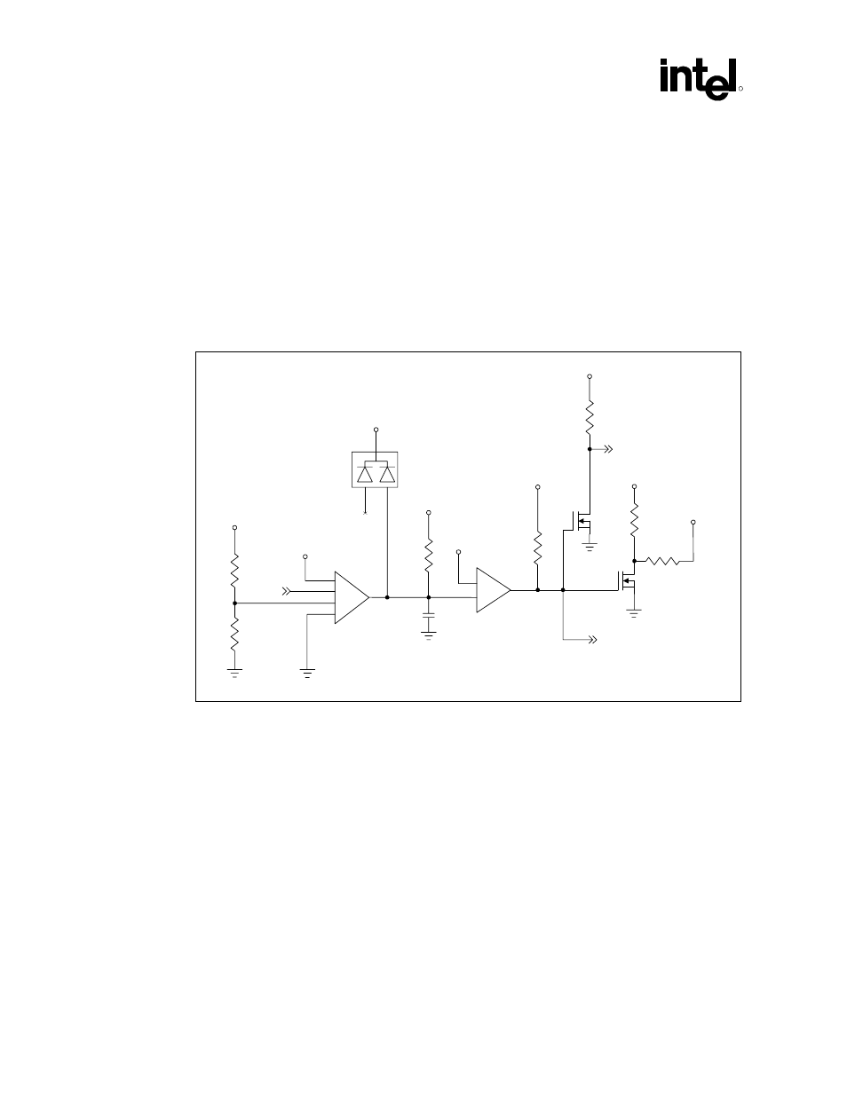
Configuring Non-VTT Processor Pins
When asserted, the VTTPWGRD signal must be level-shifted to 12V to properly drive the gating
circuitry of the Intel
®
CK-815. Furthermore, while the VTTPWRGD signal is connected to the
VTTPWRGD pin on a future 0.13 micron socket 370 processor, on a Pentium III processor
(CPUID=068xh) or Celeron processor (CPUID=068xh) that same pin is a ground. To provide
proper functionality, a 1.0 k
Ω
resistor must be placed in series between the circuitry that generates
the signal VTTPWRGD and the processor pin VTTPWRGD. Refer to Figure 12 for an example
implementation. Voltage regulators that generate the standard VTTPWRGD signal are available.
Figure 12. VTTPWRGD Configuration Circuit
5
3
2
4
VTT
VCC5
V1_8SB
732
Ω
1%
1
Κ Ω
1%
Vcc
IN+ 1
IN- 1
Gnd
2
3
1
VCC5
VTTPW RGD_Config
1
BAT54C
V1_8SB
8
7
6
IN+ 2
IN- 2
Out 1
Out 2
VCC5
20 K
Ω
VCC5
1 K
Ω
VTTPW RGD5#
LM393 Ch2
LM393 Ch1
0.1
µ
F
VTTPW RGD
1 K
Ω
1 K
Ω
VTT
VTTPW RGD12
2.2 K
Ω
VCC12
2.0 m s delay nom inal
MOSFET N
MOSFET N
ASSERTED
LO W
NOTE:
The diode is included so that repeated pressing of the reset or power button does not cause the
capacitor to build up enough charge to circumvent the 20 ms delay.