Table 33. power sequencing timing definitions – Intel 815 User Manual
Page 151
Power Delivery
R
Intel
®
815 Chipset Platform Design Guide
151
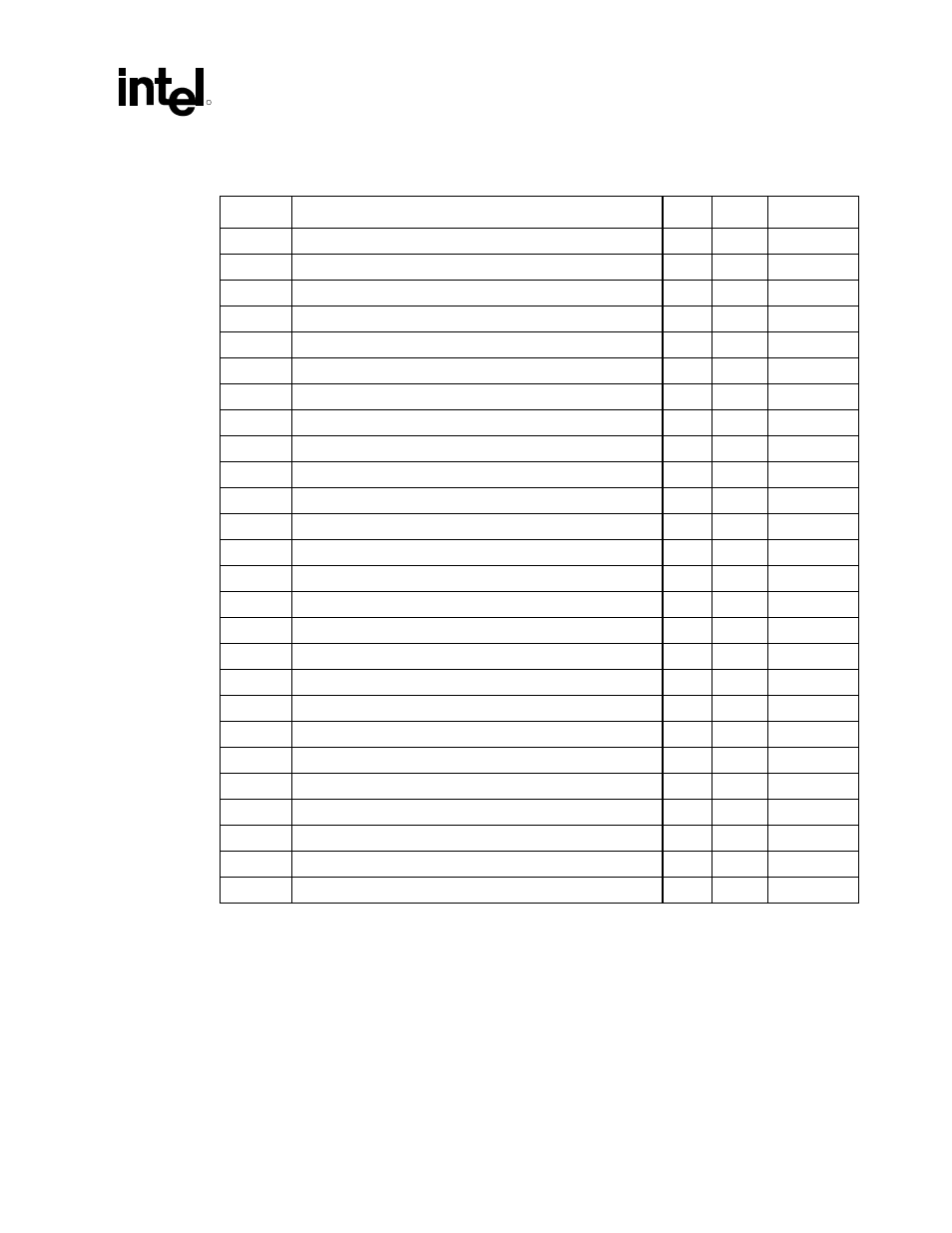
Table 33. Power Sequencing Timing Definitions
Symbol Parameter Min.
Max.
Units
t1
VccSUS Good to RSMRST# inactive
1
25
ms
t2
VccSUS Good to SLP_S3#, SLP_S5#, and PCIRST# active
50
Ns
t3
RSMRST# inactive to SLP_S3# inactive
1
4
RTC clocks
t4
RSMRST# inactive to SLP_S5# inactive
1
4
RTC clocks
t5
RSMRST# inactive to SUS_STAT# inactive
1
4
RTC clocks
t6
SLP_S3#, SLP_S5#, SUS_STAT# inactive to Vcc3.3core good
*
*
t7
Vcc3.3core good to CPUSLP# inactive
50
ns
t8
Vcc3.3core good to PWROK active
*
*
t9
Vcc3.3core good to clocks valid
*
*
t10
Clocks valid to PCIRST# inactive
500
µ
s
t11
PWROK active to PCIRST# inactive
0.9
1.1
ms
t12
PCIRST# inactive to Cycle 1 from GMCH
1
ms
t13
Cycle 1 from ICH to Cycle 2 from GMCH
60
ns
t14
PCIRST# inactive to STPCLK deassertion
1
4
PCI clocks
t15
PCIRST# to frequency straps valid
-4
4
PCI clocks
t16
Cycle 2 from ICH to frequency straps invalid
180
ns
t17
Cycle 2 from ICH to CPURST# inactive
110
ns
t18
Stop Grant Cycle to CPUSLP# active
8
PCI clocks
t19
CPUSLP# active to SUS_STAT# active
1
RTC clock
t20
SUS_STAT# active to PCIRST# active
2
3
RTC clocks
t21
PCIRST# active to SLP_S3# active
1
2
RTC clocks
t22
PWROK inactive to Vcc3.3core not good
20
ns
t23
Wake event to SLP_S3# inactive
2
3
RTC clocks
t24
PCIRST# inactive to STPCLK# inactive
1
4
PCI clocks
t25
SLP_S3# active to SLP_S5# active
1
2
RTC clocks
t26
SLP_S5# inactive to SLP_S3# inactive
2
3
RTC clocks