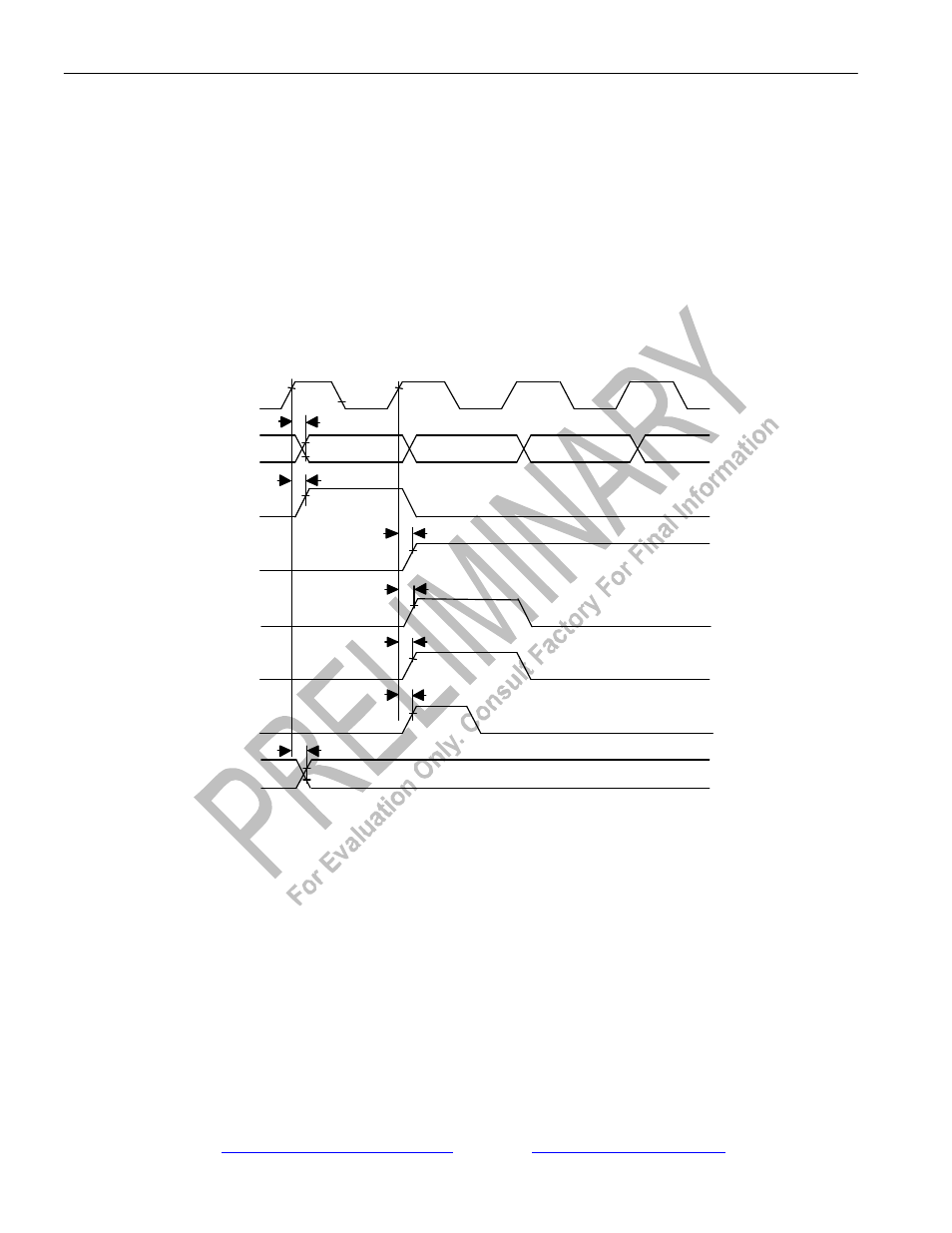
Receive side timing (t1 mode) figure 37-8 – Maxim Integrated DS21Q55 User Manual
Page 240

Product Preview
DS21Q55
240 of 248
012103
Please contact
or search
http://www.maxim-ic.com
for updated
information.
NOTES:
1) Jitter attenuator enabled in the receive path.
2) Jitter attenuator disabled or enabled in the transmit path.
3) RSYSCLK = 1.544MHz.
4) RSYSCLK = 2.048MHz.
5) RSYSCLK = 4.096MHz.
6) RSYSCLK = 8.192MHz.
7) RSYSCLK = 16.384MHz.
RECEIVE SIDE TIMING (T1 MODE) Figure 37-8
t D1
1
t
D2
RSER / RDATA / RSIG
RCHCLK
RCHBLK
RSYN
C
RLCLK
RLINK
t D1
NOTES:
1) RSYNC is in the output mode.
2) Shown is RLINK/RLCLK in the ESF framing mode.
3) No relationship between RCHCLK and RCHBLK and other signals is implied.
RCLK
RFSYNC / RMSYNC
F Bit
2
t
D2
t D2
t
D2
t D2
