Maxim Integrated DS21Q55 User Manual
Page 237
Product Preview
DS21Q55
237 of 248
012103
Please contact
or search
http://www.maxim-ic.com
for updated
information.
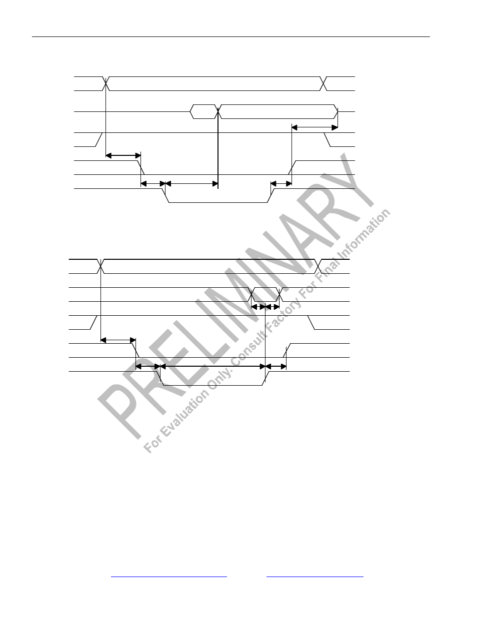
INTEL BUS READ TIMING (BTS = 0 / MUX = 0) Figure 37-4
INTEL BUS WRITE TIMING (BTS = 0 / MUX = 0) Figure 37-5
Address Valid
Data Valid
A0 to A7
D0 to D7
WR*
CS*
RD*
0ns min.
0ns min.
75ns max.
0ns min.
5ns min. / 20ns max.
t1
t2
t3
t4
t5
Address Valid
A0 to A7
D0 to D7
RD*
CS*
WR*
0ns min.
0ns min.
75ns min.
0ns min.
10ns
min.
10ns
min.
t1
t2
t6
t4
t7
t8