Functional timing diagrams, 1 t1 mode, Receive side d4 timing figure 35-1 – Maxim Integrated DS21Q55 User Manual
Page 208
Product Preview
DS21Q55
208 of 248
012103
Please contact
or search
http://www.maxim-ic.com
for updated
information.
BIT
PIN
SYMBOL
TYPE
CONTROL BIT DESCRIPTION
7
97
RFSYNC
O
6
–
RSYNC.cntl
–
0 = RSYNC is an input; 1 = RSYNC is an output
5
98
RSYNC
I/O
4
99
RLOS/LOTC
O
3
100
RSYSCLK
I
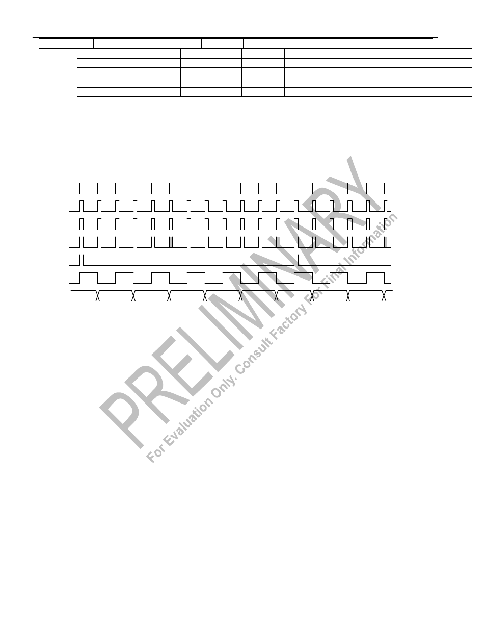
32. FUNCTIONAL TIMING DIAGRAMS
32.1 T1 Mode
RECEIVE SIDE D4 TIMING Figure 35-1
NOTES:
1) RSYNC in the frame mode (IOCR1.5 = 0) and double-wide frame sync is not enabled (IOCR1.6 = 0).
2) RSYNC in the frame mode (IOCR1.5 = 0) and double-wide frame sync is enabled (IOCR1.6 = 1).
3) RSYNC in the multiframe mode (IOCR1.5 = 1).
4) RLINK data (Fs-bits) is updated one bit prior to even frames and held for two frames.
FRAME#
1
2
3
4
5
6
7
8
9
10
11
12
1
2
3
4
5
4
RLINK
RLCLK
3
RSYNC
1
RSYNC
RFSYNC
2
RSYNC